Two-dimensional square-Au2S monolayer: A promising thermoelectric material with ultralow lattice thermal conductivity and high power factor*
2021-07-30WeiZhang张伟XiaoQiangZhang张晓强LeiLiu刘蕾ZhaoQiWang王朝棋andZhiGuoLi李治国
Wei Zhang(张伟) Xiao-Qiang Zhang(张晓强) Lei Liu(刘蕾)Zhao-Qi Wang(王朝棋) and Zhi-Guo Li(李治国)
1School of Science,Southwest University of Science and Technology,Mianyang 621010,China
2Institute of Atomic and Molecular Physics,Sichuan University,Chengdu 610065,China
3Laboratory for Shock Wave and Detonation Physics,Institute of Fluid Physics,Mianyang 610064,China
Keywords: first-principles calculations, electron-phonon interactions, lattice thermal conductivity, thermo
1. Introduction
Owing to increasingly severe environmental pollution and the depletion of fossil fuels, the search for alternative clean and renewable energy sources is urgent. Thermoelectric(TE)materials can spontaneously convert waste heat into electric energy,so they have great potential applications in alleviating the dilemmas of energy sources.[1-5]The performance of a TE material can be described by the dimensionless figure of meritZT=S2σT/(κl+κe), whereS,σ,T,κl, andκedenote the Seebeck coefficient,electrical conductivity,absolute temperature, lattice thermal conductivity, and electronic thermal conductivity, respectively. High-performance TE materials usually require both high power factor(PF=S2σ)and low total thermal conductivityκ(κ=κl+κe). Consequently, some techniques such as chemical doping,band structure engineering,strain engineering,nano-structuring,and low-dimensional structure were adopted to enhancePFor reduceκ.[6-10]Lowdimensional materials could exhibit significantly higherZTvalues than their bulk counterparts[11,12]due to the decreasedκon account of the phonon boundary scattering and the improvedPFcaused by the quantum confinement effect.
Recently, the two-dimensional (2D) transition-metal chalcogenidesM2X(M= metal andX= S, Se, Te)have attracted considerable attention due to their nontrivial properties.[13-20]Monolayerδ-Cu2S had an ultralowκlof 0.10 W/mK at 800 K, leading to a highZTof 1.33.[14]TheZTof the metal-shrouded Tl2O monolayer exceeded 3 whenT >700 K.[20]Monolayer Ag2S was also recommended as a promising 2D TE material.[17]Recently, Chenet al.[18]and Wuet al.[19]proposed a new nonmetal-shroudedM2X: monolayer square-Au2S.Its cohesive energy 3.4 eV was comparable to that of monolayer Ge(3.26 eV)and Si(3.98 eV),[21]indicating the possibility to synthesize it experimentally. Chenget al.[18]calculated the lattice thermal conductivity of this monolayer and found that it has an unusually lowκl, but the physical origins behind such a lowκlare unexplored. They also suggested that monolayer square-Au2S has ultrahigh carrier mobilities. However, the carrier mobilities of monolayer square-Au2S calculated by them were very different(their difference was more than 160%), though the same deformation potential theory was used.[22,23]This is due to the fact that the simplified phenomenological model they used contains some tunable parameters, and thus generally lacks sufficient predictive power.[24,25]Therefore, it is necessary to perform the parameter-free first-principles calculations for the electronic transport properties of monolayer square-Au2S to obtain reliable results. Furthermore, we notice that previous work focused only on carrier mobilities,the full thermoelectric transport parameters likeS,σ,κe,andPFfor deriving the figure of meritZTare still lacking.
In general, the electronic transport properties are computed in terms of the Boltzmann transport equation(BTE) within the constant relaxation time approximation(CRTA).[26-28]Actually, the carrier relaxation time relies on carrier mode, carrier concentration, and temperature.[25]Recently, the electronic transport properties could be accurately predicted by solving the parameter-free BTE under self-energy relaxation time approximation (SERTA) with the scattering limited by the electron-phonon interactions. In addition,as is well known,the spin-orbit coupling(SOC)effect may have a significant influence on the electronic band structure of materials and,further,on electronic transport properties.[29,30]Motivated by the above considerations,in this work,we aim to explore the origin of the lowκlof monolayer square-Au2S and investigate the full TE transport properties together with theZTfrom first-principles calculations and parameter-free BTE.We find that this monolayer possesses a large n-type(p-type)ZT=2.2 (1.5) at 300 K andZT=3.8 (2.5) at 600 K, indicating that it can become a highly promising room-and hightemperature TE material. Furthermore,the effects of EPIs and SOC on TE properties of the monolayer are also discussed.
2. Computational method
All first-principles calculations based on density functional theory (DFT) were performed by using the Quantum ESPRESSO package.[31]with Perdew-Burke-Ernzerhof(PBE) exchange-correlation functional.[32]The normconserving pseudopotential[33]was used to describe the corevalence interaction with a plane wave kinetic energy cutoff of 80 Ry (1 Ry=13.6056923(12) eV). The convergence threshold of 1×10⁻⁸a.u. (a.u. is short for atomic unit) for total energy and 1×10⁻⁵a.u. for forces were used. The DFT-D3 method[34]was used to take into account the long-range van der Waals interaction.The electronic band structures were calculated by the six versions of Heyd-Scuseria-Ernzerh hybrid functional (HSE06). The spin-orbit coupling (SOC) interaction was considered in the calculations of electronic band structure and phonon dispersion. Inab initiomolecular dynamics (AIMD) simulations, a 3×3×1 supercell was used as an initial structure. The timestep and total simulation time were set to be 1 fs and 10 ps,respectively. The lattice thermal conductivity can be obtained by the self-consistent solution of the BTE, as implemented in the ShengBTE package.[35]The 2nd-order interatomic force constants(IFCs)with a 5×5×1q-mesh were calculated by the density functional perturbation theory. A 3×3×1 supercell and 5×5×1k-mesh were used to calculate the 3rd-order anharmonic IFCs, and the interactions up to the eighth nearest-neighbors were included. In the BTE calculations,a denseΓ-centered 50×50×1q-mesh was adopted to obtain converged results. The vacuum lengthLis set to be 20 ˚A, which avoids the interactions between layers.For properties requiring volume normalization, an effective thickness of 6.19 ˚A was used,which includes the bucking distancehof the monolayer plus twice the van der Waals radius of a sulfur atom.[18,25,27,36,38]
The EPI matrix elements were computed by using an initial coarse 15×15×1k-mesh with a 5×5×1q-mesh,and then interpolated to a dense 150×150×1k-mesh with a 50×50×1q-mesh using the maximally localized Wannier functions, as implemented in the EPW package.[39,40]These settings are enough to ensure convergence. The energyresolved carrier relaxation time of the electronic state with band indexnand wave vectorkcan be estimated from the imaginary part of the electron self-energy Im(Σ)as follows:
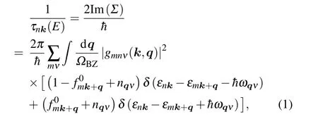
whereΩBZis the volume of the first Brillouin zone,matrix elementsgmnν(k,q)are the probability amplitude for scattering from an initial electronic state|nk〉into a final state|mk+q〉via a phononqν,fnkis the Fermi-Dirac distribution function,nqνis the Bose-Einstein distribution function,εnkis the electron eigenvalue for the state|nk〉,ωqνis the phonon frequency of wave vectorq, and branch indexν. Then, based on theτnk(E)and band structure from HSE06 with SOC,the electronic transport coefficients,includingS,σ,andκe,can be obtained as follows:
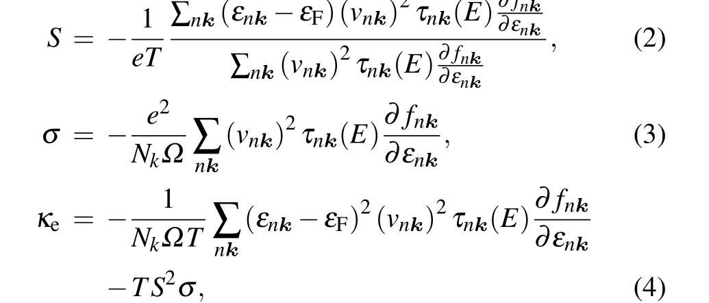
wheree,Nk,Ω,εF, andvnkrepresent the electron charge,total number ofk-points, volume of the unit cell, Fermi energy, and electron group velocity, respectively. The electronic transport coefficients were solved by using the Boltz-TraP2 package.[27]Hereinafter,we refer to this computational scheme as SOC+SERTA. To elucidate the influence of EPIs on the electronic transport coefficients,the CRTA and SERTA calculations without the SOC were carried out(referred to as NoSOC+CRTA and NoSOC+SERTA hereinafter). The role of the SOC effect is checked by comparing the SOC+SERTA calculations with the NoSOC+SERTA calculations. In the CRTA calculations, the carrier relaxation timeτwas calculated from the equation:τ=μm*/e,where carrier mobilityμand effective massm*were cited from Ref.[18].
3. Results and discussion
3.1. Structure of monolayer square-Au2S
Monolayer square-Au2S has a tetragonal structure with a space group symmetry ofP4/nmm. There are four Au atoms and two S atoms in a unit cell,and the four Au atoms are in a plane. The layer of Au atoms is sandwiched between two layers of S atoms, and each S atom is tetracoordinated with Au atoms as shown in Figs. 1(a) and 1(b). The fully optimized lattice parameter and the bucking distancehof monolayer square-Au2S are 5.74 ˚A and 2.59 ˚A,respectively. These structural parameters accord well with previous calculations.[19]The phonon dispersion and AIMD simulations indicate that the monolayer square-Au2S possesses good dynamical and thermal stability (see the supplementary material, Fig. S1).Figure 1(c) displays the electron localization functions, from which we can see that the electrons are mostly localized near S atoms,implying the ionic nature of the Au-S bond.In general,weak interatomic bonding is an indicator of lowκl.[7]

Fig.1. (a)Top view and(b)side view of the atomic structure of monolayer square-Au2S, (c) electron localization functions, and (d) high-symmetry kpoints in the first Brillouin zone.
3.2. Lattice thermal conductivity
The calculatedκlversustemperature is displayed in Fig. 2(a). As expected, monolayer square-Au2S has an ultralowκlof 0.72 W/mK at room temperature,which is smaller than other 2D nanosheets have, like SnSe,[41]Bi2Te3,[42]MoS2,[43]BP,[44]PdS2,[3]and comparable to those of the recently reported monolayers Tl2O[13]and Bi2O2Se.[6]The ultralowκlof monolayer square-Au2S is beneficial to the high TE performance. It can also be seen from Fig. 2(a) that theκlof monolayer square-Au2S decreases with temperature increasing, reaching 0.48 W/mK at 600 K. This is mainly due to the inherent enhancement of the phonon-phonon scattering with temperature increasing. It is noted that our calculatedκlof monolayer square-Au2S is lower than that in Ref. [18],which is because the van der Waals interaction exerts influence on group velocity and the phonon relaxation time is included in the present work. The calculated contributions from different phonon branches toκlin Fig. 2(b) reveal that lowfrequency acoustic branches contribute to the majority of theκl. In contrast, the contribution from high-frequency optical branches is quite small.
According to phonon Boltzmann theory,κlis proportional to the phonon lifetime and the square of the group velocity.[28]Thus, to understand the origin of such an ultralowκl, the phonon group velocities and relaxation timeversusfrequency are shown in Figs. 2(c) and 2(d), respectively. The group velocities and phonon lifetime from the acoustic branches are higher than those from the optical branches, which helps explain why the contribution from acoustic branches accounts for the majority ofκl. The maximum phonon group velocity of all phonon modes for monolayer square-Au2S is quite small(within 3 km/s),resulting in the lowκl. On the other hand, the phonon lifetimes for the acoustic modes are low enough(1 ps-100 ps), which implies the strong phonon scattering. The anharmonic phonon scattering can be characterized by two parameters: the Gr¨uneisen parameterγand the size of the three-phonon scattering phase spaceW. The mode Gr¨uneisen parameter and weighted phase space of three-phonon scattering of the acoustic branches are both large(see Fig.S2 in Supplementary material),leading to low phonon lifetime and,hence,lowκl.
It is worth noting that EPIs may have an important effect on phonon thermal conductivity.[45,46]However, the present calculations elucidate that the phonon relaxation time arising from the intrinsic phonon-phonon scattering is at least two orders of magnitude smaller than that from electron-phonon scattering (see Fig. S3 in supplementary material). Therefore, according to Matthiessen’s rule,[28]theκlof monolayer square-Au2S due to EPIs can be safely ignored.
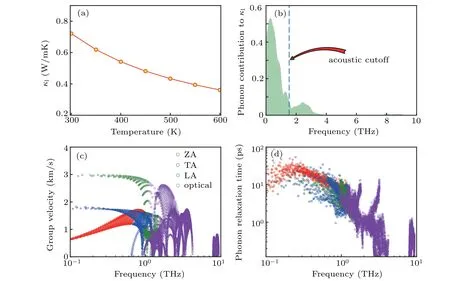
Fig.2. (a)Lattice thermal conductivity κl versus temperature,(b)contribution of phonons at different frequencies to κl,and(c)phonon group velocity,and(d)phonon relaxation time versus frequency at 300 K for monolayer square-Au2S.
3.3. Electronic transport and TE properties
Monolayer square-Au2S with lowκlwill be a highly useful TE material if itsSandσare high enough. The electronic transport properties depend mainly on the band structure and carrier relaxation time. We use the hybrid functional HSE06 to overcome the underestimation of bandgap by PBE.As shown in Fig.3(a), monolayer square-Au2S is a semiconductor with a direct bandgap of 0.8 (1.2) eV with (without)SOC,which is slightly smaller than that reported in Ref.[19].The projected density of states shown in Fig. 3(b) indicate that both Au atoms and S atoms contribute to states near the Fermi level, implying that there is a strong hybridization between orbitals of Au and S atoms. Further analyses of the orbital-resolved density of states(see Fig.S4)indicate that the states near the valence band maximum(VBM)are contributed mainly by the hybridization of atomic orbitals of Au atoms and atomic orbitals of S atom. The states around the conduction band minimum (CBM), however, stem mainly from the atomic orbitals of the Au atom. Consequently, the valence band and conduction band may have different dispersion characteristics as shown in Fig.3(a).There exists strong dispersion near the CBM,while the bands around the VBM are relatively flat. Upon the introduction of the SOC effect,the band edges near the VBM become more dispersive,while the band shape around the CBM is hardly affected. Therefore, after including SOC, the band edges around the Fermi level are highly dispersive, leading to small effective mass (m*=0.06mefor electron andm*=0.10mefor hole[19]). According to the deformation potential theory, the carrier mobilityμis inversely proportional to effective massm*. And the electronic conductivityσcan be calculated from the equation:σ=μne,wherenis carrier concentration. Thus,the small effective mass will result in largeμandσ,thereby a high power factor.
The carrier relaxation time can be accurately calculated from the EPI matrix elements. According to Eq.(1), the carrier relaxation time and EPI matrix elements are related by the electron self-energy Im(Σ). The projections of Im(Σ)on the band structure and the energy-dependent carrier relaxation time are displayed in Figs. 3(a) and 3(c), respectively. States with small Im(Σ)appear around the VBM and CBM because electrons and holes near the band edges are less scattered as a result of the limited phase space.[7,47]Moreover, a strong energy dependence can be witnessed from the energy-dependent carrier relaxation time as shown in Fig.3(c).The carrier relaxation time decreases uniformly with temperature increasing.The relaxation time at 300 K is higher than that at 600 K.This can be easily understood, since more and more phonons are populated with the increase of temperature, which leads the electron-phonon scattering to strengthen.[48]
Figure 4 shows the curves of electronic transport and TE parametersversuscarrier concentrations at 300 K for n-type and p-type dopings under the SOC+SERTA.Figures 4(a)and 4(b) display the largeSvalues for n-type and p-type doped monolayer square-Au2S.For instance,the absolute value ofSfor n-type(p-type)doping at the optimal carrier concentration(corresponding to the maximumZT)is 265 μV/K(214 μV/K).Both of them are in the range of 200 μV/K-300 μV/K,which is an indicator of good TE material.[1,49]Figures 4(c)and 4(d)show that theσfor n-type doping is superior to that for p-type doping. Notably, the absolute value ofSis inversely proportional to carrier concentration, whereas theσfollows the opposite trend,suggesting that there is a trade-off between them,leading to a maximumPFat a certain carrier concentration.

Fig. 3. (a) Electronic band structure calculated by HSE06 functional with (solid line) and without considering the SOC effect (gray dotted line), (b)projected density of states with considering SOC effect, and (c) energy-dependent carrier relaxation time τnk(E). Band structure with SOC effect is color-coded according to Im(Σ)at 300 K,which is scaled by color bar with units of eV.

Fig.4. Curves of electronic transport and TE coefficients versus carrier concentration of n-type(left panels)and p-type(right panels)doped monolayer square-Au2S at 300 K: ((a), (b)) absolute value of Seebeck coefficient S, ((c), (d)) electrical conductivity σ, ((e), (f)) power factor PF, and ((g),(h))figure of merit ZT.
The calculatedPFvalues in Figs. 4(e) and 4(f) shows that the maximumPFof n-type doping is twice that of p-type doping mainly due to the higherσfor n-type doping. The n-type (p-type) doped monolayer square-Au2S has an exceptionalPF=9.90(4.85) mW/mK2at 300 K, which is higher than that of monolayersδ-Cu2S and Bi2O2Se. The calculatedκefor n-type (p-type) doping at optimal concentration is 0.38 (0.20) W/mK, which is lower thanκl. Moreover, theκefor n-type (p-type) doping contributes only 34% (21%) to the totalκ(see the supplementary material, Fig. S5). Owing to the highPFand quite lowκ, the n-type (p-type)ZTof 2.2(1.5)can be achieved at the optimal hole concentrationnE≈4.0×1010cm-2(nH≈1.1×1011cm-2)andT=300 K as shown in Figs.4(g)and 4(h).
Figure 5 displays the contour map ofZT versustemperature and doping concentration under SOC+SERTA.It is found that the maximumZTand the optimal carrier concentration both increase with temperature increasing. The maximum ntype (p-type)ZTexceeds 3.7 (2.4) atnE≈8.5×1010cm-2(nH≈4.0×1011cm-2) and 600 K. The maximum n-typeZT= 3.8 is higher than that of typical bulk TE material:SnSe (2.6).[50]and 2D monolayers:δ-Cu2S (1.33),[14]Tl2O(3.35),[20]and Bi2O2Se(3.35).[6]

Fig.5. Contour map of ZT as a function of temperature and carrier concentration of(a)n-type and(b)p-type doped monolayer square-Au2S.
3.4. Effects of SOC and EPIs on TE properties
The SOC effect and EPIs may play a vital role in determining the electronic properties of materials.[25,30,51,52]The influence of the SOC effect can be revealed by comparing the results from SOC+SERTA and NoSOC+SERTA calculations as shown in Fig. 4. With the consideration of SOC, for ptype doping,Sdecreases whereasσincreases significantly,which can be understood through the above analyses of band structures. Since the increase ofσis dominant,the maximumPFandZTwith SOC are~4 times and~3.5 times larger than the results without SOC,respectively. Moreover,the optimum hole concentration decreases by nearly two orders of magnitude with SOC strengthening. On the other hand, the band edges around CBM are less affected by the SOC effect as shown in Fig. 3(a). Therefore, forSandσof n-type doping, the difference between the results with and without the SOC effect is much smaller than the counterparts in the case of p-type doping. Moreover, the maximum values of n-typePFandZTwith and without the SOC effect are close to each other(see the left panel of Fig.4).
To reveal the influence of EPIs on the electronic transport properties, we compare the results from SERTA and CRTA calculations in Fig. 4. For n-type and p-type dopings, theSfrom SERTA reasonably accords with that from CRTA,which indicates the low correlation betweenSand carrier relaxation time. The discrepancy between the CRTA and SERTA results is apparent forσ,κe,and the maximum values ofPFandZT,which are shown in Fig. 4 and Fig. S5. The maximum values ofPF(ZT) from SERTA are~56% (28%) and~90%(84%)lower than those from CRTA for n-type and p-type dopings,respectively. Therefore,the strong energy dependence ofτnk(E)plays an essential role in determining the overall electronic transport and TE performance.The completely different treatment of carrier relaxation time is responsible for the discrepancy.In the CRTA calculations,the carrier relaxation time is regarded as a constant. It is calculated by the deformation potential theory, which only considers the electron-acoustic phonon scattering. However,for monolayer square-Au2S,the optical phonon scattering is comparable to that from the acoustic phonon branches (see Fig. S6 in the supplementary material). The SERTA adopts the energy-resolved carrier relaxation time deduced from the EPI matrix elements which take into account all electron-phonon scattering processes.To date,the electronic transport and TE properties of several materials,including Li,[53]Si,[29,30]GaAs,[29]SnSe,[52]Mg3Sb2,[24]CoSi,[51]etc. have been investigated by the parameter-free algorithm and the calculation results accord well with the experimental data. Therefore,the electronic transport and TE properties of monolayer square-Au2S obtained by the SERTA are believed to be more predictive than by the CRTA,although the corresponding experimental data are not available at present.In addition,although the maximum values ofPFandZTfrom the SERTA seriously deviate from those from the CRTA, the optimum carrier concentrations predicted by the two methods are relatively close to each other.
4. Conclusions
In summary, thermal, electronic transport, and thermoelectric properties of monolayer square-Au2S are systematically investigated via a parameter-freeab initioBoltzmann transport algorithm. Owing to the low group velocity and strong anharmonic phonon scattering, the monolayer square-Au2S possesses an ultralow lattice thermal conductivityκlof 0.72 W/mK at 300 K. The square-Au2S monolayer has extraordinarily high Seebeck coefficient and electrical conductivity. Consequently, the maximum power factor of the ntype(p-type)square-Au2S monolayer can be as large as 9.90(4.85)mW/mK2at 300 K.Benefiting from the ultralowκland the high power factor,a high room-temperature figure of meritZTof 2.2(1.5)can be achieved for n-type(p-type)doping,and it increases up to an ultrahigh value of 3.8 (2.5) at 600 K. In addition,when EPIs are considered,theZTvalues are significantly reduced by 28%(84%)for n-type(p-type)doping. After introducing the SOC effect, the p-typeZTis substantially increased by 3.5 times but the n-type one is almost unaffected.Our analyses strongly suggest that the 2D square-Au2S monolayer could be a potential candidate for future-generation TE applications.
Acknowledgment
The calculations were carried out on TianHe-2 at the LvLiang Cloud Computing Center in China.
猜你喜欢
杂志排行

Chinese Physics B的其它文章
- Projective representation of D6 group in twisted bilayer graphene*
- Bilayer twisting as a mean to isolate connected flat bands in a kagome lattice through Wigner crystallization*
- Magnon bands in twisted bilayer honeycomb quantum magnets*
- Faraday rotations,ellipticity,and circular dichroism in magneto-optical spectrum of moir´e superlattices*
- Nonlocal advantage of quantum coherence and entanglement of two spins under intrinsic decoherence*
- Universal quantum control based on parametric modulation in superconducting circuits*