Vertical polarization-induced doping InN/InGaN heterojunction tunnel FET with hetero T-shaped gate∗
2021-05-24YuanHaoHe何元浩WeiMao毛维MingDu杜鸣ZiLingPeng彭紫玲HaiYongWang王海永XueFengZheng郑雪峰ChongWang王冲JinChengZhang张进成andYueHao郝跃
Yuan-Hao He(何元浩), Wei Mao(毛维),‡, Ming Du(杜鸣), Zi-Ling Peng(彭紫玲), Hai-Yong Wang(王海永),Xue-Feng Zheng(郑雪峰), Chong Wang(王冲), Jin-Cheng Zhang(张进成), and Yue Hao(郝跃)
Key Laboratory of Ministry of Education for Wide Band-Gap Semiconductor Materials and Devices,School of Microelectronics,Xidian University,Xi’an 710071,China
Keywords: InGaN TFET,hetero T-shaped gate,polarization-doped source and drain
1. Introduction
As the size of semiconductor devices continues to shrink into the nanoscale, the problems of short channel effects(SCEs)and off-state leakage in traditional MOSFETs are becoming more and more serious. Especially due to thermal emission mechanism,the subthreshold slope(SS)cannot break through the limit of 60 mV/decade,which is not suitable effectively for energy-efficient and low-voltage applications.[1–4]Tunneling field-effect transistors (TFETs) have been considered as a suitable alternative to nanoscale MOSFETs in future low power electronics applications.[1]Based on the quantum band-to-band tunneling(BTBT)mechanism,TFETs could realize steeper average subthreshold swing (SSavg<60 mV/decade), lower off-state leakage current (IOFF), and great immune to short channel effects in comparison with conventional nanoscale MOSFETs.[5–7]
However, there still exist many problems needed to be solved during the application of TFETs with conventional physical doping, such as the high thermal budget and expensive annealing techniques due to ion-implantation physical doping,and the random dopant fluctuation(RDF),which can deteriorate the device performances.[8–12]Recently, various dopingless TFETs have been proposed based on the chargeplasma concept,[13–16]which demonstrates an effective way to realize TFETs without physical doping. And based on the polarization effect near III-nitride-based heterointerfaces,[17–21]the lateral polarization-induced InN-based TFETs (PI-InNTFET) have been demonstrated by our group.[22]This also opens a new path to the further development of TFETs without physical doping processing. In addition, in order to improve the on-state current, some effective methods, such as gate engineering,energy band engineering,and source-pocket doping[23–30]have been proposed and investigated.
In this paper, a novel vertical polarization-induced doping InN/InGaN heterojunction tunnel FET with hetero Tshaped gate (InN-Hetero-TG-TFET) is proposed and investigated. This device features a polarization-doped drain and source combined with a hetero T-shaped gate, which is different from the conventional vertical tunnel FET with physical doping. Based on these features, the problems about the random dopant fluctuation and the high thermal annealing techniques could be avoided, and the on-state performance could be improved. Comparative analyses between the InN-Hetero-TG-TFET and the vertical polarization-induced doping InN/InGaN heterojunction tunnel FET with homo Tshaped gate (InN-Homo-TG-TFET) are conducted. And the systematical simulations of the influence of the work-function and position of hetero T-shaped gate on the performance of the InN-Hetero-TG-TFET are carried out by Silvaco-Atlas.These results demonstrate the excellent characteristics of the InN-Hetero-TG-TFET in comparison with the InN-Homo-TG-TFET and our reported lateral polarization-induced InNbased TFET(PI-InN-TFET),which indicates a great potential of the proposed InN-Hetero-TG-TFET in the low power applications.
2. Device structure and simulation parameters
Figure 1 shows the schematic cross-section of InNHomo-TG-TFET (Fig. 1(a)) and InN-Hetero-TG-TFET(Fig. 1(b)). The T-shaped gate and dual channel are used in both devices,and both the devices have the same main dimensions. The main parameters of the InN-Homo-TG-TFET and proposed InN-Hetero-TG-TFET are shown in Table 1. Both devices use the vertical InN/InxGa1−xN/InN layer structure to form the drain and source region without physical doping. Furthermore, the source and drain are set to be at both sides of devices, which is compatible with the planar fabrication process of the GaN-based HEMTs. The InN-Hetero-TG-TFET features a hetero T-shaped gate consisting in two metals with different metal work-functions applied to modulate the InxGa1−xN band between hetero gate at different gate bias voltages,which could be used to control the tunneling distance and thus improving the on-state current and reducing the ambipolar leakage current.
Devices are simulated with two-dimensional numerical software Silvaco-Atlas. A Poisson’s equation is used to solve self-consistently the carrier current continuity equations. Device models in this paper are mainly based on our early research.[16,22,31]The nonlocal BTBT model is used for the consideration of the spatial variation of the energy band and the more accurate calculation of the tunneling process. The Shockley–Read–Hall and Auger recombination models are adopted to consider the effect of carrier recombination. Besides, band-gap narrowing model, concentration-dependent and field-dependent mobility models are also used. Main material parameters in simulations are given in Table 2.

Fig.1. Schematic cross-section of(a)InN-Homo-TG-TFET and(b)InN-Hetero-TG-TFET.
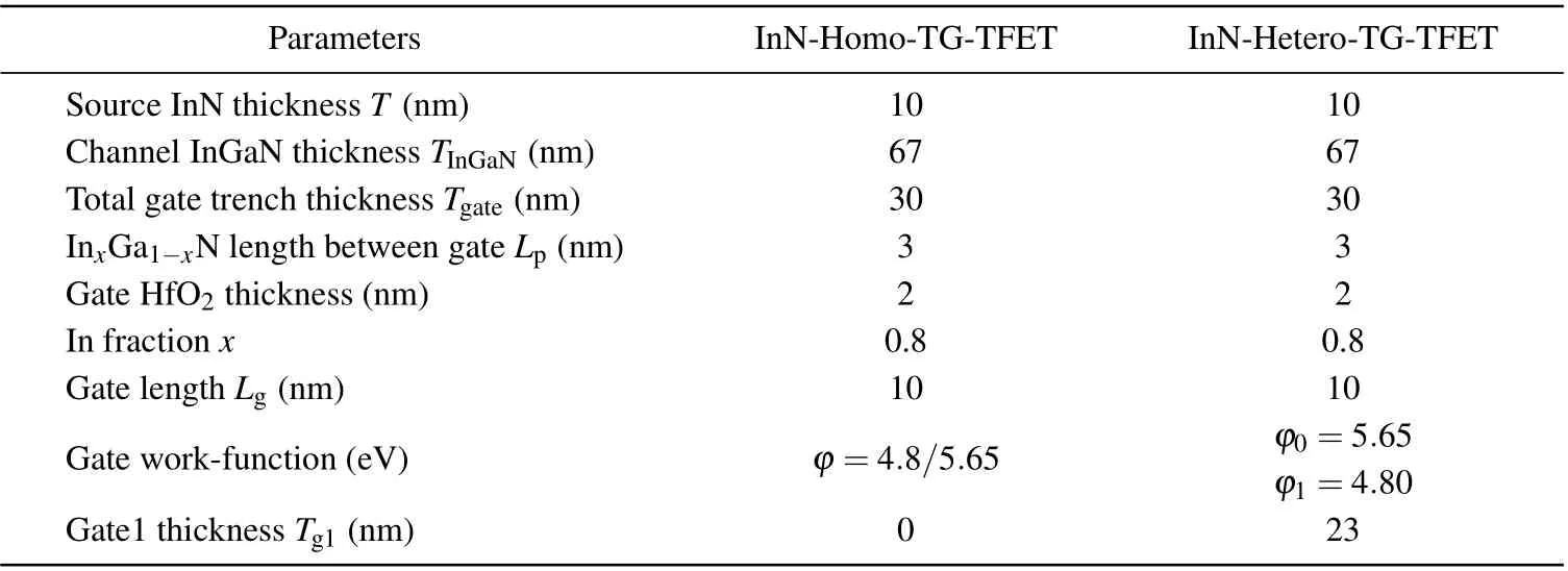
Table 1. Design parameters used in simulations.

Table 2. Material parameters in simulations.[17,32,33]
The detailed distributions of the polarization-induced carrier concentration in the InN-Hetero-TG-TFET can be observed in Fig. 2. As shown in the figure, the source region exhibits the P-type doping with the peak hole concentration near the top InN/InGaN junction, while the drain region exhibits the N-type doping with the peak electron concentration near the bottom InGaN/InN junction. Figure 3 displays the vertical distribution diagram of carrier concentration and polarization charge concentration in the source region and drain region corresponding to Fig.2 along the line D–in Fig.1(b).As shown in Fig. 3, there is a great negative polarization charge density peak σtopnear the top InN/InGaN junction because of the spontaneous and piezoelectric polarization effect,which indicates a large number of net negative bound polarization charges are located near the junction. Based on the local neutralization principle,holes are consequently induced to neutralize these negative bound sheet charges, which thus forms the P-type doping of source region. A positive polarization charge density peak σbottomappears near the bottom In-GaN/InN junction,and thus the electrons can be induced near the bottom InGaN/InN junction in the same way,which forms N-type doping of drain region. The results are consistent with experimental results reported previously.[34]

Fig.2. Distribution of polarization-induced(a)hole concentration(Conc.) and(b)electron concentration in InN-Hetero-TG-TFET.
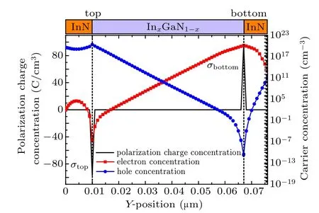
Fig.3. Vertical distribution of carrier concentration and polarization charge concentration in source region and drain region along line D–in Fig.1(b).
3. Results and discussion
3.1. Device performance of InN-Homo-TG-TFET and proposed InN-Hetero-TG-TFET
Figure 4 shows the transfer characteristic curves of the InN-Homo-TG-TFET (ϕ = 5.65 eV), InN-Homo-TG-TFET(ϕ = 4.8 eV), and proposed InN-Hetero-TG-TFET (ϕ0=5.65 eV, ϕ1=4.8 eV). As can be seen, both InN-Homo-TGTFETs exhibit almost the same transfer characteristic curves,which is due to the fact that the change of work-function of the gate in the InN-Homo-TG-TFET can nearly only affect the threshold. Compared with the InN-Homo-TG-TFET,the InNHetero-TG-TFET shows a high IONof 4.45×10⁻⁵A/µm at VDS=0.5 V and Voverdrive=0.5 V.And,an IONof more than 10−4A/µm can be achieved in the InN-Hetero-TG-TFET at VDS=0.5 V and Voverdrive=1 V.Besides,the calculated SSavgof the InN-Hetero-TG-TFET is 7.5 mV/dec which is much smaller than that of the InN-Homo-TG-TFET(39.4 mV/dec).As shown in the figure, all the three devices have almost the same good off-state characteristics, which lead to a higher ION/IOFFof 1013in the InN-Hetero-TG-TFET than that in the InN-Homo-TG-TFET (with ION/IOFFof 1011) at Voverdrive=0.5 V.These results demonstrate that the device with a hetero T-shaped gate possesses an excellent turn-on performance.
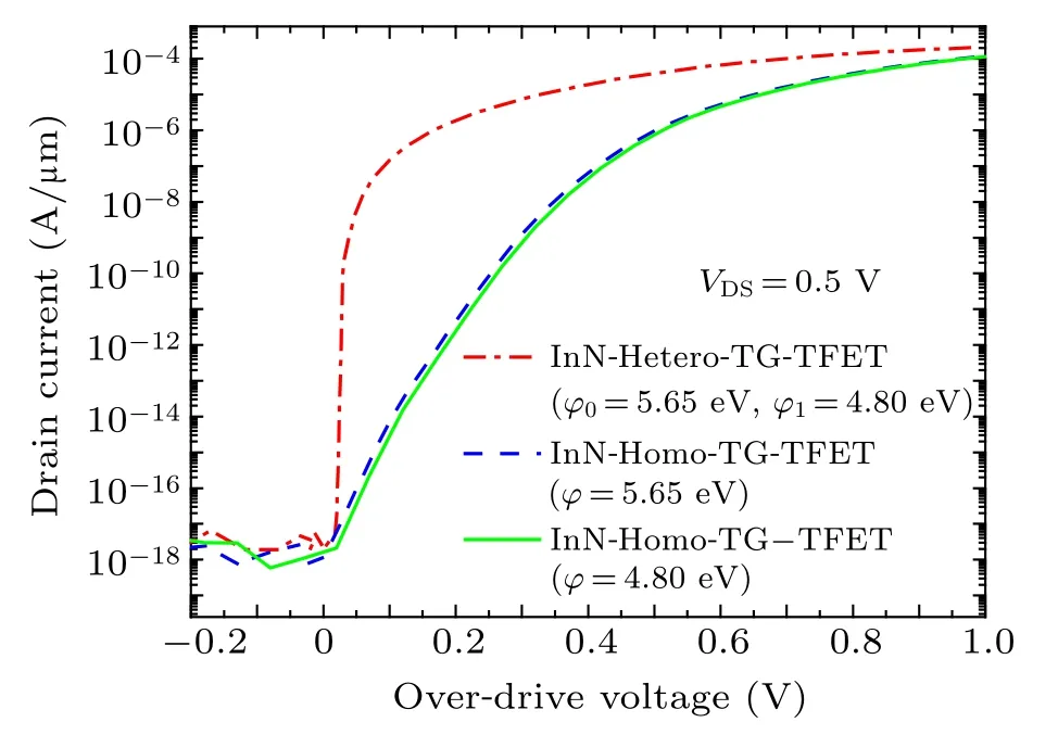
Fig. 4. Transfer characteristic curves of InN-Homo-TG-TFET (ϕ =5.65 eV), InN-Homo-TG-TFET (ϕ =4.8 eV), and proposed InN-Hetero-TG-TFET(ϕ0=5.65 eV,ϕ1=4.8 eV).
In order to reveal the tunneling mechanism of the proposed InN-Hetero-TG-TFET, figure 5 gives the contour of the nonlocal BTBT e-tunneling rate in the right half part of the InN-Homo-TG-TFET and proposed InN-Hetero-TGTFET. As shown in Fig. 5, comparing with the InN-Homo-TG-TFET, a wide tunneling region along the line E–in Fig.1(b)can be realized in the InN-Hetero-TG-TFET,which results in a wider one-dimensional tunneling rate profile in Fig.6.And from Fig.6 it is seen that the tunneling rate peak in the InN-Hetero-TG-TFET is much larger than that in the InNHomo-TG-TFETs near the interface of InN/InGaN. Besides,the introduction of gate 1 can play an effective role in improving the tunneling rate near the bottom of gate trench in the InN-Hetero-TG-TFET.Because the integral of the area under each tunneling rate curve can represent the value of the tunneling current,the greater area under the tunneling rate curve in the InN-Hetero-TG-TFET indicates a greater tunneling current than in the InN-Homo-TG-TFET.
Fig. 5. Contours of nonlocal BTBT e-tunneling rate of half part of (a) InN-Homo-TG-TFET and (b) proposed InN-Hetero-TG-TFET when Voverdrive=0.5 V and VDS=0.5 V.
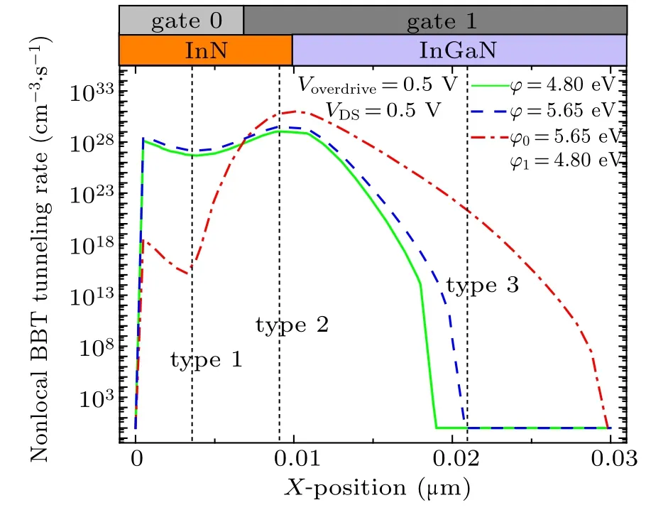
Fig. 6. One-dimensional distribution of nonlocal BTBT tunneling rate extracted from InN-Homo-TG-TFET (ϕ =5.65 eV), InN-Homo-TG-TFET (ϕ = 4.8 eV), and proposed InN-Hetero-TG-TFET (ϕ0 =5.56 eV,ϕ1 =4.8 eV)when Voverdrive =0.5 V and VDS =0.5 V along the line E–in Fig.1(b).
In Fig. 5(b), there exist three typical types of tunneling paths in the InN-Hetero-TG-TFET.For the convenience of the analysis afterwards,the three typical types of tunneling paths are marked in Figs. 5(b) and 6, namely, along the line A–(type 1),line B–(type 2),and line C–(type 3)corresponding to Fig.1(b). The type 1 and type 2 describe the tunneling from InN to InGaN under the control of gate 0 and gate 1,respectively. And the type 3 describes the tunneling path in InGaN under the control of gate 1.
Further explanation about the modulation mechanism of the hetero T-shaped gate is shown by Fig. 7. The arrowed lines represent the tunneling paths and tunneling distances in devices at on-state. Almost the same energy band of the InNHomo-TG-TFETs with ϕ =5.56 eV or ϕ =4.8 eV can be seen,indicating the slight effect of the metal work-function on the performance. This is consistent with the result in Fig.4.
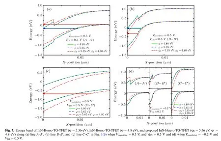
In Fig.7,in all devices,the tunneling distances of type 2 are all less than 5 nm which are obviously smaller than those of types 1 and 3. It indicates a dominant effect of type 2 on the tunneling current. Because of the effective modulation effect of the hetero T-shaped gate,the tunneling distance of type 2 in the InN-Hetero-TG-TFET is shorter than that in the InN-Homo-TG-TFET,resulting in a greater tunneling rate and thus a larger tunneling current as well as a smaller average subthreshold swing in the InN-Hetero-TG-TFET.This accords well with the results in Figs.4 and 6. Besides,nearly no tunneling can be seen for type 3 in InN-Homo-TG-TFETs,while there still exits a certain tunneling for type 3 in the InN-Hetero-TG-TFET,which further demonstrates an effective modulation effect of the bottom of gate trench in InN-Hetero-TG-TFET on the energy band. In Fig.7(d),nearly no tunneling can be seen in all devices at off-state,which indicates a significantly small off-state leakage current. These results demonstrate excellent characteristics of the InN-Hetero-TG-TFET.
3.2. Influence of hetero T-shaped gate1 work-function ϕ1 on InN-Hetero-TG-TFET
Figure 8 shows the influence of hetero gate1 workfunction ϕ1on transfer characteristics in InN-Hetero-TGTFET. As shown in the figure, the transfer curves shift towards the negative voltage direction when ϕ1decreases. And with the help of hetero gate, the SSavgand IONcan be improved efficiently. The variation extracted from Fig. 8(a) is shown in Fig. 8(b) and the corresponding energy band diagrams are also depicted in Fig.9. It could be seen in Fig.8(b)that IONcontinuously increases while SSavgdecreases with ϕ1decreasing. The results can be illustrated by the energy band diagrams in Fig.9. As it is shown,the tunneling distance decreases with ϕ1decreasing and reaches a minimum value at ϕ1=4.70 eV,which results in a highest ION. And,due to the improved modulation ability of the gate with ϕ1decreasing,the SSavgkeeps on falling. In order to achieve the enhancement mode device,ϕ1=4.8 eV is chosen as the optimal value in the following.

Fig. 8. Influence of hetero gate-1 work-function ϕ1 on InN-Hetero-TG-TFET performance,showing(a)transfer characteristics and(b)extracted ION and SSavg.
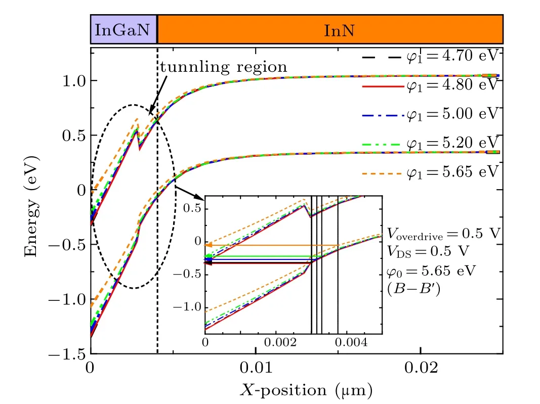
Fig. 9. Influence of hetero gate-1 work-function ϕ1 on energy band of InN-Hetero-TG-TFET along line B–in Fig. 1(b) when VDS =0.5 V and Voverdrive=0.5 V.
3.3. Influence of hetero T-shaped gate-0 work-function ϕ0 on InN-Hetero-TG-TFET

Fig. 10. Influence of hetero gate-0 work-function ϕ0 on InN-Hetero-TG-TFET performance: (a) transfer characteristics and (b) extracted ION and SSavg.
Figure 10 shows the influence of hetero gate-0 workfunction ϕ0on transfer characteristics in the InN-Hetero-TG-TFET. As it is shown, the transfer curves shift towards the negative voltage direction and the subthreshold characteristics are degraded gradually as ϕ0decreases. The variation extracted from Fig.10(a)is shown in Fig.10(b),and the corresponding energy band diagrams are also depicted in Fig.11.It could be seen in Fig. 10(b) that IONdecreases and SSavgincreases with ϕ0decreasing, which is attributed to the increase in tunneling distance as shown in Fig. 11. Therefore,ϕ0=5.56 eV is adopted in the following investigation.
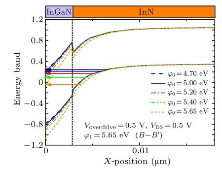
Fig. 11. Influence of hetero gate-0 work-function ϕ0 on energy band of InN-Hetero-TG-TFET along line B–in Fig. 1(b) when VDS =0.5 V and Voverdrive=0.5 V.
3.4. Influence of hetero T-shaped gate position Tg1 on InNHetero-TG-TFET
The influence of hetero gate-1 thickness Tg1on the performance of InN-Hetero-TG-TFET is shown in Fig. 12 and the corresponding energy band diagrams are shown in Fig.13.As shown in Fig.12,the transfer curves shift towards the negative voltage direction when Tg1is raised. And IONincreases continuously with Tg1increasing. Based on the energy band in Fig. 13, the energy band on gate side will shift down with Tg1increasing, which can shorten the tunneling distance and increase the tunneling rate,resulting in the variation of ION. It can be observed that SSavgfirst decreases and then increases but reaches a minimum value at Tg1=23 nm. This is due to the changing of modulation ability of the hetero gate around Tg1=23 nm. With Tg1increasing, the modulation ability of the whole hetero gate(gate 0 and gate 1)converts from that of the high metal work-function homo gate to that of hetero gate,then to that of the low metal work-function homo gate,which results in the trend of SSavg. Based on these analyses,it is important to find the balance point of Tg1, and Tg1is chosen to be 23 nm for the proposed device in this paper. The characteristics of the proposed device in comparison with those of our previous reported lateral PI-InN-TFET and the state-of-the-art III-nitride-based TFETs are given in Table 3, which demonstrates the excellent performance of InN-Hetero-TG-TFET.

Fig.12. Influence of hetero gate-1 thickness Tg1 on InN-Hetero-TG-TFET performance for total gate trench thickness Tgate of 30 nm,showing(a)transfer characteristics and(b)extracted ION and SSavg.
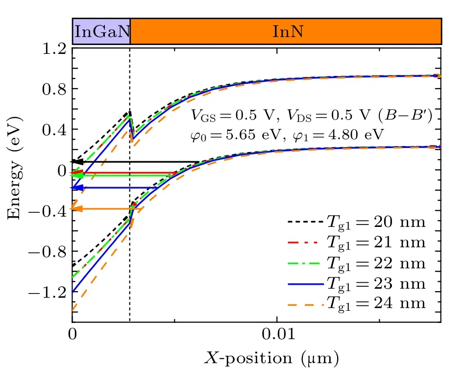
Fig.13. Influence of hetero gate-1 thickness Tg1 on energy band along line B–in Fig.1(b)when VDS=0.5 V and VGS=0.5 V.

Table 3. Comparison of characteristic between proposed device and state-of the-art nitride TFETs.
4. Conclusions
In this paper, we present a new vertical polarizationinduced doping InN/InGaN heterojunction tunnel FET with hetero T-shaped gate (InN-Hetero-TG-TFET). The proposed device can realize the drain and source region doping by means of polarization effect without the conventional physical doping processing, which can avoid the random dopant fluctuation (RDF) and the problems related to the high thermal annealing techniques in the conventional physical doping tunnel FETs. In addition, the improvement of the IONand SSavgcan be achieved,benefitting from the utilization of the hetero T-shaped gate with different metal work-functions. The device electrical characteristics and the physical mechanisms are studied systematically. Simulation results demonstrate the excellent performance of InN-Hetero-TG-TFET in comparison with those of the InN-Homo-TG-TFET and our previously reported lateral polarization-induced InN-based TFET(PI-InNTFET), which could provide an effective method for the further development of TFETs.
猜你喜欢
杂志排行

Chinese Physics B的其它文章
- Corrosion behavior of high-level waste container materials Ti and Ti–Pd alloy under long-term gamma irradiation in Beishan groundwater*
- Degradation of β-Ga2O3 Schottky barrier diode under swift heavy ion irradiation*
- Influence of temperature and alloying elements on the threshold displacement energies in concentrated Ni–Fe–Cr alloys*
- Cathodic shift of onset potential on TiO2 nanorod arrays with significantly enhanced visible light photoactivity via nitrogen/cobalt co-implantation*
- Review on ionization and quenching mechanisms of Trichel pulse*
- Thermally induced band hybridization in bilayer-bilayer MoS2/WS2 heterostructure∗