Tunable valley filter efficiency by spin–orbit coupling in silicene nanoconstrictions*
2021-05-24YiJianShi施一剑YuanChunWang王园春andPengJunWang汪鹏君
Yi-Jian Shi(施一剑), Yuan-Chun Wang(王园春), and Peng-Jun Wang(汪鹏君)
College of Electrical and Electronic Engineering,Wenzhou University,Wenzhou 325035,China
Keywords: valley polarization,spin–orbit coupling,quantization,silicene
1. Introduction
Valleytronics has received considerable interests since the discovery of hexagonal two-dimensional materials.[1]Two inequivalent valleys located at the corners of Brillouin zone in honeycomb lattice provide a new degree of freedom for electrons,which can be used for information storage and processing. Among various valleytronic devices, valley filter and valley valve[2–5]are the most fascinating application for future electronics. Valley filters are realized in quantum point contact,[6,7]and other structures with nanobubble,[8,9]domain wall,[10,11]Corbino nanodisk[12,13]or Weyl semimetals.[14,15]In addition, mechanical,[16–18]optical,[19–21]magnetic[22–24]and electrical[25–27]methods have been applied to process valley information.
Nevertheless, it has not been extensively discussed how spin–orbit coupling (SOC) controls the valley polarization.The SOC is rather weak in graphene,while relatively strong in silicene and counterpart of other group IVA elements such as germanium and tin,due to a low-buckled structure. The SOC can be artificially engineered by adatoms or substrates,as well as changing the amplitude and stretch direction of strain.[28–31]The energy gap induced by SOC at Dirac points leads to quantum spin Hall (QSH) effect.[32–34]In this topological phase,the electronic edge state with time-reversal invariance conducts charge and spin at the sample boundaries without dissipation,which is robust against the interference of impurities and disorders.[35–37]As external staggered electric field is applied to a silicene system with a critical strength,a topological phase transition from QSH phase to trivial insulator phase occurs and the bandgap opens. To utilize this topological phase transition, topological field effect transistors have been proposed to rapidly switch between on- and off-states by tuning staggered electric field.[34,38]Furthermore, with external exchange field applied, high efficiency spin valley filters have been reported in strained silicene systems.[39,40]However,valley-dependent transport properties solely affected by larger SOC without breaking the inversion symmetry of hexagonal lattice system is still unclear and worthy of study.
In this work, we theoretically investigate the valley filter efficiency controlled by SOC in silicene nanoconstrictions.The edge orientation of the silicene lattice is zigzag type throughout the constriction. We focus on the effect of SOC that plays a vital role in manipulating the valley-dependent transport in a valley filter device. External staggered electric field and exchange field are not applied in our system, which keeps the valley filter working in QSH phase. The paper is organized as follows. In Section 2,the model and methods are introduced. Results and analysis are presented in Section 3.Conclusions are given in Section 4.
2. Model and methods
Valley filter device was originally proposed in graphene nanoconstriction made up of wide-narrow-wide quantum point contact.[2,3]The analogous nanoconstriction structure consisting of zigzag silicene nanoribbons is illustrated in Fig.1. The whole open system is composed of three parts: left lead,central device,and right lead.The symmetrical structure has gradual tapers with zigzag edges at the interface between leads and central device. The widths of the lead and central device are denoted by WZand WC,respectively. Meanwhile,L is the length of the channel in the central device and a=3.86 ˚A is the lattice spacing of silicene.
The Hamiltonian of the system can be described by the next-nearest-neighbor tight-binding model as follows:[29,32,34]
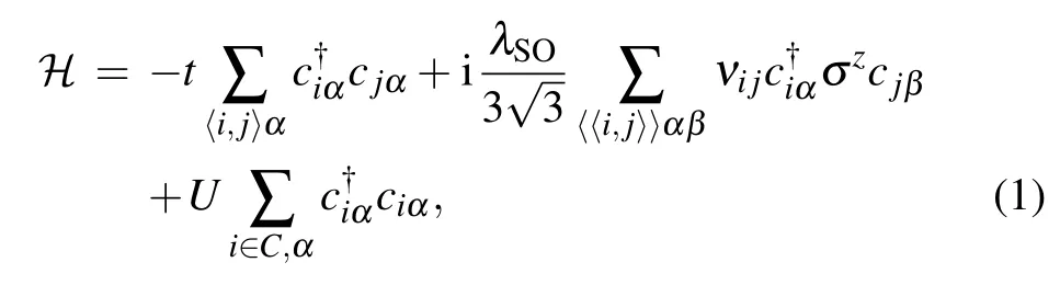
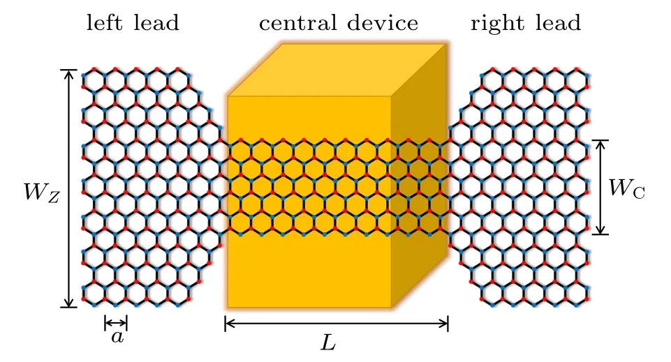
Fig. 1. Geometry of silicene nanoconstriction acting as a valley filter consists of quantum point contact with zigzag edges. It is decomposed into three parts: left lead,central device,and right lead. The widths of the lead WZ tapers down gradually to that of central device WC. The length of the constriction is L and lattice spacing of silicene is a. Homogeneous electric field is applied at the central device region(yellow block)to switch polarity of the valley filter.
At low temperature limit, the valley-resolved conductance GK/K′of the silicene nanoconstriction for K/K′valley is given by the Landauer formula,
where tmn,αis the transmission amplitude from the incident channel n to the outgoing channel m for electrons with spin α. The channel index n goes through all the modes in two valleys and m is only counted for the modes in a single K/K′valley. The total conductance G=GK+GK′is the sum of the two valley-resolved conductance. With the Hamiltonian of the system obtained from Eq.(1),the retarded Green function for central device together with two interface parts can be defined by GrD=(EI −HD−ΣL−ΣR)−1,where HDis the Hamiltonian matrix with its dimension equal to the number of atoms inside the corresponding area,E is Fermi energy and I is the identity matrix. The self-energy ΣL/ΣRof the left/right infinite lead can be calculated by the recursive Green function method.[7,41,42]The detailed transmission amplitude tmn,αin terms of Fermi energy E and electrostatic potential U is then accessible by employing Green’s function into the modematching method.[30,43–45]The procedure starts from solving a quadratic eigenvalue equation derived from the Schr¨odinger equation to get real (complex) values of wave number for propagating(evanescent)modes,as well as the corresponding wavefunction. For propagating modes,the group velocities of Bloch waves are also calculated to distinguish the directions of propagation (left-going and right-going). Then the propagating modes are sorted into two groups (K and K′valleys),according to their wave number belonging to(0,π/a)or(π/a,2π/a). Finally,the detailed transmission amplitudes of different valleys are calculated with the wavefunction and Green’s function.
With valley-resolved conductance calculated, the valley polarization of transmitted current can be written as
where perfect valley filter efficiency P=±1 indicates that the propagating modes allowed in the system are fully at the K/K′valley.
3. Results and discussion
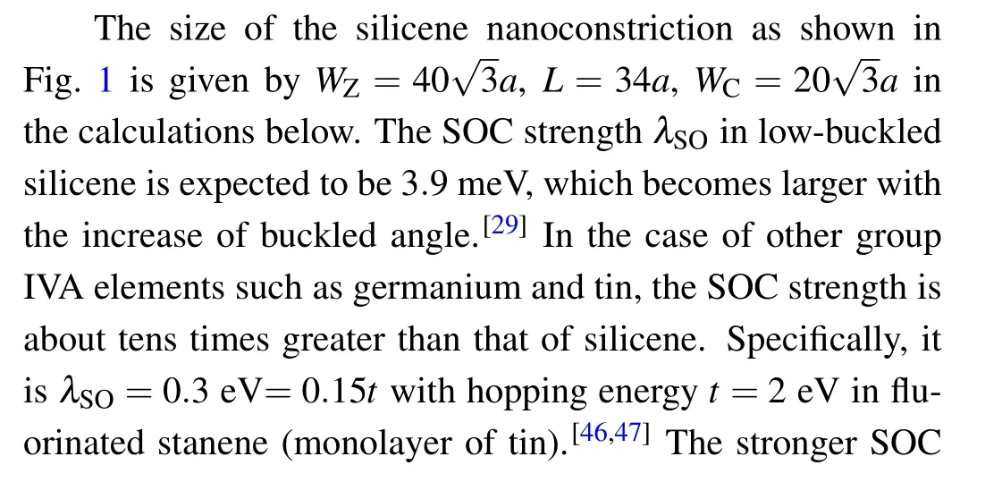

Fig.2.The bandstructure in the left lead,central device and right lead of the silicene nanoconstriction atµ0=0 with spin–orbit coupling strength(a) λSO =0, (b) λSO =0.06t, (c) λSO =0.12t. The Fermi energy is EF=t/3 and homogenous electrostatic potential is U =t/3 at the central device region. The energy spacings between the lowest modes and Fermi energy at the two valleys in the central device (half the energy gap between conductance band and valence band at K/K′ point) are denoted by ∆,∆1 and ∆2,respectively.


Fig. 3. The four lowest eigenvalues at K/K′ point in the bandstructure of the central device as a function of spin–orbit coupling strength λSO. The magnitude of λSO is in units of the nearest neighbour hopping energy t. The energy spacings ∆, ∆1, ∆2 are also found in the bandstructure of the central device.
The total conductance G and valley-resolved conductance GK, GK′ as a function of the electrochemical potential µ0are depicted in Figs.4 and 5,respectively. As shown in Fig.4,the plateaus of quantized conductance G=(2N+1)×2e2/h at positive µ0holds on,even as SOC is considered. Here N is a non-negative integer and 2N+1 represents the total number of propagating modes in the central device. The widths of conductance plateaus are determined by the energy spacing of the subbands at K or K′point in the central device. Especially,the first conductance plateau of the graphene-like case in the positive region (3∆) is broadened due to SOC, which is related to the second lowest subband energy in Fig. 3. In addition,the resonance dip of the total conductance in the negative µ0region in the graphene-like case is flattened by SOC because quasi-bound state in the valence band[2]turns into robust QSH edge state. In Fig.5(a),GKand GK′ in the graphene-like case show good valley selectivity at small µ0. The first conductance step appears atµ0=3∆for both GKand GK′,where the channel of the second subband in the central device opens. In Figs.5(b)and 5(c),instead of step-like plateaus,both GKand GK′show smooth variation at smallµ0due to the existence of SOC. This means that the propagating modes in both valleys participate in the electronic transport. The turning points for GKand GK′to quantized conductance plateaus are at µ =∆1and ∆2for λSO=0.06t and 0.12t, respectively,which are related to the sudden change of group velocity at K or K′point for the QSH edge state in the bandstructure of central device as shown in Fig.2.
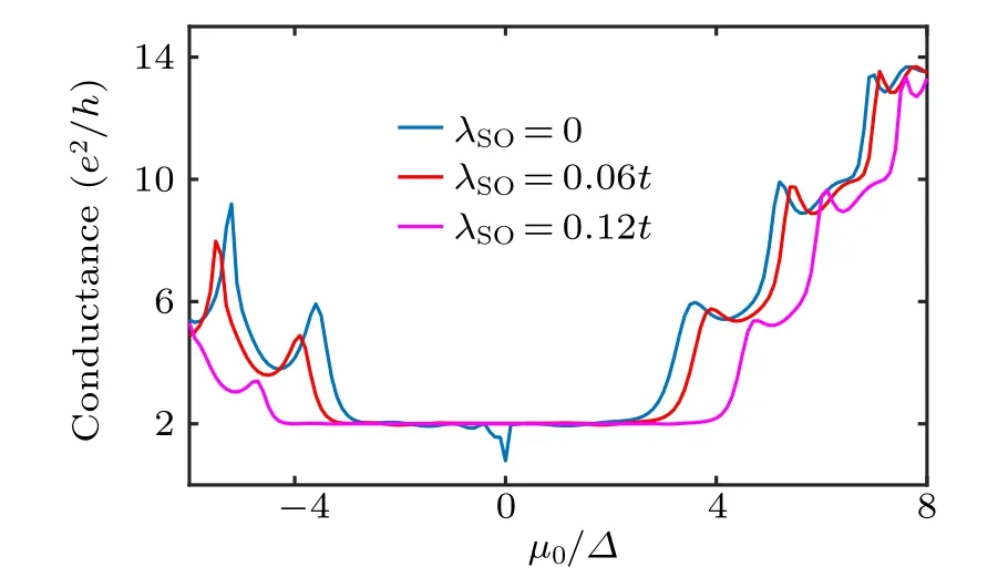
Fig.4. Total conductance G as a function of the electrochemical potential µ0 for the silicene nanoconstriction. The modes are spin degenerated and the unit of conductance is e2/h. The magnitude ofµ0 is scaled by ∆. The blue, red and magenta lines denote the case of spin–orbit coupling strengths λSO=0,λSO=0.06t,and λSO=0.12t,respectively.
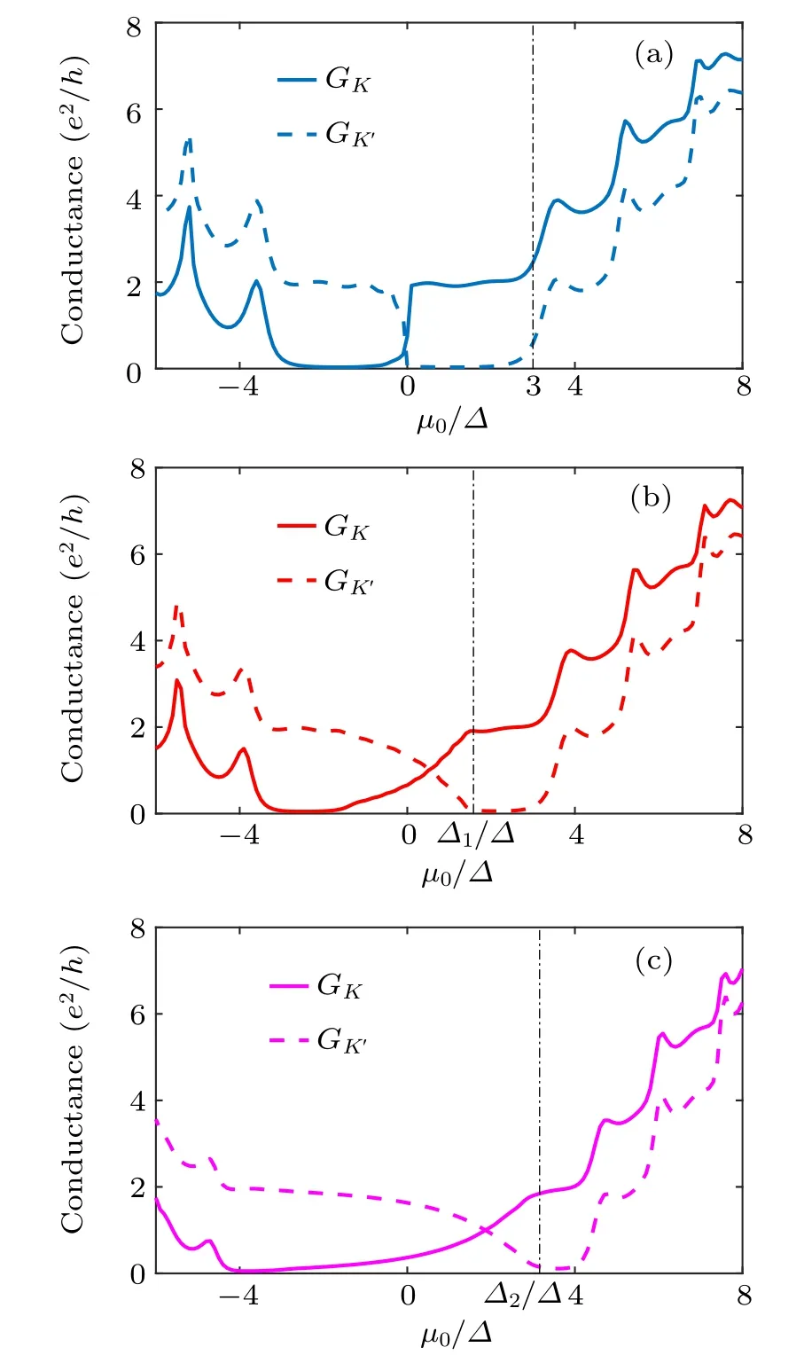
Fig. 5. Valley-resolved conductance GK (full line) and GK′ (dashed line) as a function of the electrochemical potential µ0 for the silicene nanoconstrictions. The blue, red and magenta lines denote the case of spin–orbit coupling strengths (a) λSO = 0, (b) λSO = 0.06t, (c)λSO=0.12t,respectively.
The valley polarization as a function of the electrochemical potentialµ0is depicted in Fig.6. As a positiveµ0is tuned larger than the eigenvalue of lowest subband at K or K′point in the central device,the polarization shows fractional plateaus P = 1/(2N+1). The ratio of two valley-resolved conductances is GK′/GK=N/(N+1), where N and N+1 are the number of propagating modes for K′and K valley in the central device, respectively. The perfect valley filter efficiency P=1 is achieved as only one right-going propagating channel in the K valley is allowed in the central device, which is the case of N = 0. Compared with the graphene-like case,the polarization plateaus is shifted as SOC is strengthened,which corresponds to the conductance step shown in Fig. 4.At smallµ0with only the QSH edge state allowed as the channel in the central device, the polarization changes smoothly for λSO=0.06t and λSO=0.12t, instead of a abrupt transition of polarization reversal for λSO=0. Therefore, in the presence of SOC,consecutively tunable valley filter efficiency from negative to positive values can be achieved by aligning the homogenous electric field in the central device. Larger SOC improves the resolution of valley polarization under the same increment of electrochemical potential.
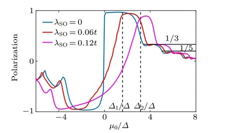
Fig. 6. Valley polarization as a function of the electrochemical potentialµ0 for the silicene nanoconstriction.The blue,red and magenta lines denote the case of spin–orbit coupling strengths λSO=0,λSO=0.06t,and λSO=0.12t,respectively.
The valley polarization at µ0=0 becomes smaller than zero for λSO= 0.06t, and even smaller for λSO= 0.12t,which means GK′dominates the valley filter efficiency with SOC considered. This phenomenon can be intuitively explained by matching the propagating modes at two separate valleys in the leads and the QSH edge state channel in the central device. Take the case of λSO= 0.12t as an example. The zoomed-in bandstructure of the leads is shown in Fig. 7(a), where the right-going propagating modes are labeled in two magenta boxes. The modes lying in the region of(4π/3a,2π/a) for the K valley are labeled by n=0,1,...,7 from the right-most to the left-most, and the modes lying in the region of (2π/3a,π/a) for the K′valley are labeled by n=−1,−2,...,−7 from the right-most to the left-most.Among all the propagating modes, those in the K′valley are closer to Γ point than in the K valley, which have greater possibilities to transmit through the central device. To be specific, the mode-detailed spin-degenerate conductances for each propagating mode are shown in Fig.7(b). The modes in the K valley (G0,G1,...,G7in top two rows) have little contribution to conductance at µ0=0. In contrast, the modes in the K′valley(in bottom two rows,especially G−1,G−2,G−3)show greater conductances at µ0=0. Consequently,the sum of conductances for the modes in the K′valley(GK′)is greater than that of the K valley (GK) as shown in Fig. 5, leading to negative polarization.
This behavior demonstrates that valley-mixed scattering exists in the valley filter with SOC taked into accounted. In addition, larger SOC in the system makes the group velocity of QSH edge state channel faster at the central device. Therefore,the modes at K′valley are more and more conductive atµ0=0 with the increase of SOC,resulting in smaller negative polarization. Moreover, nearly full valley filter efficiency is also reached at the first plateau as nonzero SOC exists. The critical values ofµ0for the valley polarization growing to the first plateaus are ∆1and ∆2for λSO=0.06t and 0.12t respectively, where the Fermi energy goes through the Dirac point of the QSH edge state in the central device. At larger µ0,the silicene nanoconstrictions have almost the same valley filter effect as the graphene-like case, except the plateaus shift depending on the strength of SOC.

Fig.7. (a)The zoomed-in bandstructure for the leads at Fermi energy EF =t/3(dashed line)with spin–orbit coupling strength λSO =0.12t.Two magenta boxes are depicted to separate the right-going propagating modes in the K and K′valleys.The modes in the K valley are labeled by n=0,1,...,7 from the right-most to the left-most,and the modes in the K′valley are labeled by n=−1,−2,...,−7 from the right-most to the left-most. (b)Mode-detailed spin-degenerate conductances(in units of e2/h)for the right-going propagating modes in the leads as a function of the electrochemical potential µ0 (in units of ∆). The conductances (full line) in top two rows are for the K valley and the conductances(dashed line)in bottom two rows are for the K′ valley.
4. Conclusion
In summary, we have studied valley-dependent transport properties controlled by SOC in silicene nanoconstrictions. The valley polarization calculated by numerical method shows remarkable valley filter effects as the graphene-like case. However, SOC leads to valley-mixed scattering in silicene nanoconstrictions,which provides consecutively tunable and wide-range valley filter efficiency around Dirac point with only QSH edge state mode allowed in the channel. The lowest conductance step is both flattened and broadened due to SOC,implying robust charge transport in zigzag-edge silicene nanoconstrictions.As the homogeneous gate potential is gradually tuned,quantized conductance steps and valley polarization plateaus are obtained. The position and length of the plateaus are determined by the strength of SOC. Generally,similar valley filter behavior should also be found in devices constructed by other group IVA elements such as germanium and tin. The models proposed here are versatile for different elements with different bond parameters and geometries. Our work may provide insights for designing valleytronic devices with tunable valley filter efficiency by SOC.
杂志排行

Chinese Physics B的其它文章
- Corrosion behavior of high-level waste container materials Ti and Ti–Pd alloy under long-term gamma irradiation in Beishan groundwater*
- Degradation of β-Ga2O3 Schottky barrier diode under swift heavy ion irradiation*
- Influence of temperature and alloying elements on the threshold displacement energies in concentrated Ni–Fe–Cr alloys*
- Cathodic shift of onset potential on TiO2 nanorod arrays with significantly enhanced visible light photoactivity via nitrogen/cobalt co-implantation*
- Review on ionization and quenching mechanisms of Trichel pulse*
- Thermally induced band hybridization in bilayer-bilayer MoS2/WS2 heterostructure∗