High-throughput identification of one-dimensional atomic wires and first principles calculations of their electronic states*
2021-05-24FengLu卢峰JintaoCui崔锦韬PanLiu刘盼MeichenLin林玫辰YahuiCheng程雅慧HuiLiu刘晖WeichaoWang王卫超KyeongjaeChoandWeiHuaWang王维华
Feng Lu(卢峰), Jintao Cui(崔锦韬), Pan Liu(刘盼), Meichen Lin(林玫辰), Yahui Cheng(程雅慧), Hui Liu(刘晖),Weichao Wang(王卫超), Kyeongjae Cho, and Wei-Hua Wang(王维华),†
1Department of Electronic Science and Engineering,and Tianjin Key Laboratory of Photo-Electronic Thin Film Device and Technology,Engineering Research Center of Thin Film Optoelectronics Technology(Ministry of Education),Nankai University,Tianjin 300350,China
2Department of Material Science and Engineering,the University of Texas at Dallas,Richardson,75080,USA
Keywords: high-throughput calculation, one-dimensional atomic wires, electronic structure, first principles calculation
1. Introduction
Low dimensional van der Waals (vdW) materials are more flexible in designing electronic devices with high performance.[1,2]Since the discovery of graphene in 2004,the low dimensional materials[3–14]such as graphene and other two-dimensional (2D) materials,[3–12]one-dimensional(1D) materials like carbine[13]and metal trihydride MH3[14]have attracted extensive attention. Different from threedimensional (3D) bulks, the low dimensional systems possess a variety of unconventionally physical properties owing to unique band structures, charge screenings, and electron–phonon couplings modulated by the dimensionality.[15–18]For instance, 3D diamond, 2D graphene, and 1D carbine display completely distinguished properties owing to their different hybridization orbitals under different dimensions. Especially for 1D quantum materials,their potential applications in nanoelectronics,spintronic devices,and sensors are promising because they reach the physical limit scale of the electronic materials with periodic crystal structures. Thus,exploring realistic 1D quantum materials and unveiling their properties have been one of the central and significant topics in fields of condensedmatter physics and materials science.
Among 1D materials, one special kind of systems can be defined as 1D atomic wires (AWs) because their width is in few-atoms scale. In the past two decades, 1D AWs have demonstrated rich and unique properties, such as Peierls transition,[19,20]spin–charge separation,[21]Tomonaga–Luttinger liquids,[22]strongly quantum fluctuation,[23]and superconductivity.[24]Meanwhile,the electronic properties would change with the dimension reduction. For instance, the band gap type of 1D Sb2S3and Nb2Se9shows a transition from indirect to direct with the dimension reduction from 3D to 1D.[25,26]Moreover,the conducting property from metallic to semiconducting takes place in Mo6Te6with the dimension reduction to 1D.[27]From the viewpoint of magnetic properties, 1D AW of CoH3is a half-metal with 100% spin-polarization.[14]1D Mn/Fe-benzenetetramines are bipolar magnetic semiconductors, which could be modulated into half metals by carrier doping.[28]In addition, thermoelectric and catalytic performances of ultrafine 1D AWs would also be improved.[29–31]Therefore,1D AW materials are more suitable to be applied in high-performance sensors,transistors,catalysts,etc.[30–33]
Similar to exfoliating graphene from graphite, the 1D AWs could be exfoliated from the vdW bulks. Although preliminary classification on vdW bulk materials has been reported by Cheon et al. in 2017[34]and the progress on some 1D materials has been achieved, few excellent 1D AW candidates could be practically applied in devices due to lack of enough reliable 1D AWs. To solve this issue,the comprehensive database of 1D AWs is urgently required to be established based on 3D solid crystal database. Moreover, the stabilities,exfoliating feasibilities, and electronic properties of 1D AWs are demanded to be examined and provided.Without the direct connection between the reliable 1D AWs and their electronic properties, it severely limits the fundamental explorations on 1D AWs and their practical applications in devices. Herein,the detailed classifications on 367 kinds of potential 1D AW candidates and systematic investigations on their geometrical structures,electronic structures,possibly magnetic properties,and stabilities have been performed. At the meanwhile, all computational results are stored in the database with format of JavaScript Object Notation(JSON),which provides a comprehensive 1D AW candidate resource and a significant platform for the scientific community to further undertake theoretical analysis, experimental verification, and practical applications in devices using suitable 1D AW systems.
2. Computational methods and usage notes of the database
In this work, all the calculations were performed based on density functional theory (DFT) within Vienna ab initio simulation package (VASP).[35]The generalized gradient approximation (GGA) with Perdew–Burke–Ernzerhof(PBE) functional was adopted for the exchange–correlation potential.[36]Considering the weak vdW interactions between inter-wires in bulk materials,the Grimme’s DFT-D3 approach was involved.[37]For 1D AWs, the vacuum thickness was set as 30 ˚A in order to minimize the interaction between periodic AWs. The plane-wave cutoff energy was set as 500 eV in all of the calculations. All the atomic positions were fully optimized to converge until the force on each atom was less than 0.02 eV/˚A with the fixed bulk lattice constants along the wires. In the electronic structure calculations,the energy convergence was set as 10−5eV.In order to investigate the structural stability of 1D AWs,phonon dispersions were studied by using Phonopy code based on the interface with VASP.[35,38,39]
All the computational results, including the structures,electronic structures, magnetic states, and stabilities of 367 1D AW candidates, are compiled in the supplementary materials (SM) in PDF format. To help researchers easily search some specific information from a large amount of data, these results are also stored in the database with format of JavaScript Object Notation(JSON).For the JSON format file, three nested layers of objects are included, where one can extract the required information according to the keys in each layer. The database are openly available at http://www.dx.doi.org/10.11922/sciencedb.j00113.00004.
3. Results and discussion
3.1. Screening and identification of 1D atomic wires
In order to obtain the potential 1D AWs, the possible 1D AW candidates can initially be explored by sweeping 3D crystal structure databases, such as Inorganic Crystal Structure Database (ICSD),[40,41]Materials Project (MP)database,[42]etc. The primary task is to discriminate the vdW bulk materials from the databases. In other words, how to distinguish the vdW interaction is the key issue. One of the common methods to identify the vdW interaction is through comparing the distance(d)of two atoms with the sum of their covalent bond radii, which effectively identifies 2D and 1D vdW solids and 2D/1D heterostructures materials by Cheon et al.[34]After tremendous screening of the possible vdW bulks list[34]combined with the latest MP database[42](https://materialsproject.org)using data mining algorithm,the possible 1D AWs have been obtained. Meanwhile, it is required that the bond length along the 1D AW direction is smaller than the shortest distance between two nearest interwires in the parent bulk phase. Moreover,the f-electrons systems are not considered here since they could not be accurately described by GGA[36]or local density approximation(LDA)[43]based on DFT. Consequently, 367 1D AW candidates are obtained and considered in this work.
The structure,electronic structure,and stability information of 1D AWs are compiled in SM in PDF format. For facilitating the scientific researches to extract some specific information from a large amount of data in SM,an additional SM in JSON format is also provided. For the JSON format file,three nested layers of objects are included, where one can extract the required information according to the keys in each layer.Table 1 summarizes the keys corresponding to the objects in each layer. For example, one can get the structural information of 1D AW AuBr through the keys‘Binary 1D AWs’and‘AuBr’. It is worth noting that all the figures are encoded with Base64 format. Besides, a python code is also offered as an example to extract the data from the JSON file. To run the python code, the python relevant packages like json module and base64 module are required to be pre-installed.
Based on the 1D vdW parent materials,a statistical classification and analysis is presented in Fig. 1. In terms of the crystal structure classification in Fig.1(a),it is found that the systems with monoclinic and orthorhombic symmetries hold~37% and ~39%, respectively. The system with triclinic symmetry is ~10%,and other systems only hold smaller proportions with ~5% for tetragonal, ~6% for hexagonal, and~3%for trigonal. Based on the point group distribution,it is found that the majority of ~34% is 2/m, followed by mmm with ~31%. A complete list of the crystal structure information among our predicted 367 1D AW materials is provided in SM.Figures 1(b)and 1(c)display the chemical formula types and composition species of these 1D AWs. Among them,halides,chalcogenides,and pnictides are partially overlapped.In details,248 halides account for a large proportion of ~68%since their valence state of −1 is easier to be satisfied. Besides,230 chalcogenides and 111 phosphides exist in Fig.1(c).Moreover,123 binary and 176 ternary compounds are the major parts with ratios of 34%and 48%in Fig.1(b).Furthermore,according to the chemical formula prototypes in Fig.1(b),the major format is AB2,which is followed by AB3,ABC3,AB4,ABC,etc.
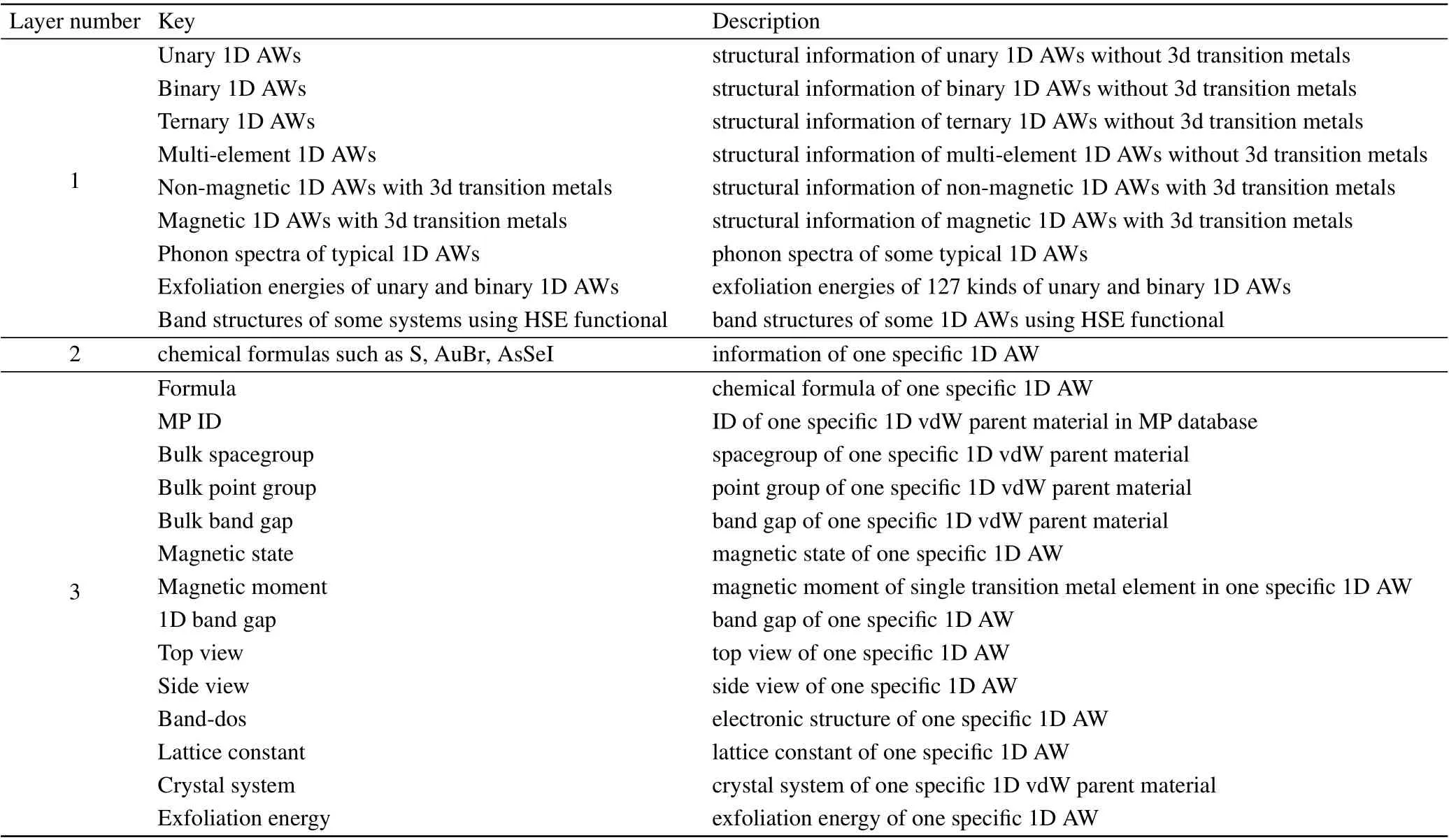
Table 1. Description of keys in JSON file.
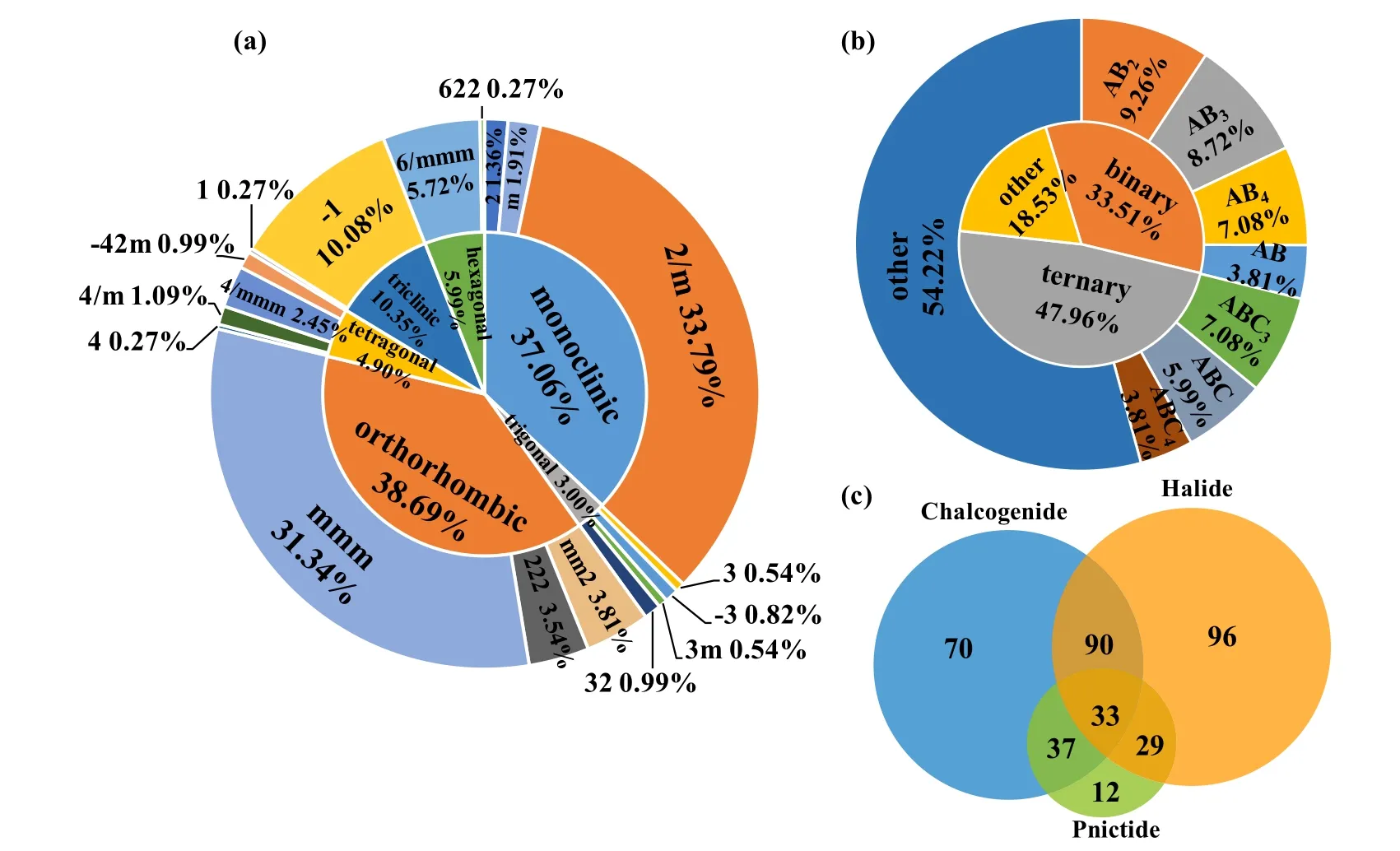
Fig.1.Statistics on 1D vdW parent materials.Classification of 1D vdW bulk materials in terms of(a)crystal structures and point groups,(b)species of chemical elements and chemical formula prototypes,(c)chemical compositions.
3.2. Electronic structures and magnetic properties of some specific 1D atomic wires
With the dimension reduction, the electronic properties of 1D AWs may demonstrate evident changes relative to 3D bulks. 1D BeCl2and 1D SnCl2as typical 1D AWs show the band gap type transition and the band gap reduction compared with 3D bulks, respectively. In details, the bulk BeCl2is an indirect band gap semiconductor, but it turns into a direct band gap semiconductor for 1D AW in Fig. 2(a), implying that 1D BeCl2would be used in sub-nm optoelectronic devices. In general, 316 semiconductors and 51 metals are present among 367 kinds of 1D AWs, whose detailed band structures and density of states(DOS)are provided in the SM.Since the electronic correlation effect on the band structures could not be accurately described by GGA-PBE functional,the band gaps are usually underestimated. Thus, more accurate method such as Heyd–Scuseria–Ernzerhof (HSE) functional or GW correction is required to produce more accurate band structures and band gaps.As shown in Fig.S1 in SM,the band gap of the semiconducting 1D AW BPS4increases with HSE functional compared with those using GGA-PBE functional, and the metallic character of ICl2and Ta4SiTe4using HSE functional is maintained. Even for the transition metal compounds like MoCl3O,the band gap is still absent and the metallic band structure is preserved after the HSE functional is considered. Thus, the qualitatively properties of most systems reported here may not change much in this work. In fact,the GW correction or dynamical mean field theory (DMFT)should be considered to obtain more accurate electronic states of transition metal compounds in further studies. From the vdW bulk materials to 1D AWs, several evident changes occur in the electronic structures owing to the bond length variation and the symmetry lowering,which deserves further thorough investigations. For most of 1D semiconducting AWs,the band gaps of most 1D AWs are enlarged compared with their bulks owing to the conventionally quantum confinement effect,which is basically induced by the reduced electronic interaction between the inter-wires. In contrast, some 1D AWs in the SM demonstrate decreased band gaps compared to the bulks. Taking SnCl2as an example in Fig. 2(b), the band gap of bulk SnCl2is 3.15 eV,but it shrinks to 2.95 eV for its 1D AW.The band gap reduction results from the bond length reduction of Sn–Cl from bulk to 1D AW.
The 1D magnetism is also a significant topic in the low dimensional materials, especially among 3d transition metal compounds. As listed in Table 2, the stable magnetic configurations of 1D AWs with 3d transition metal elements have been explored through comparing the energies of nonmagnetic, ferromagnetic (FM), and N´eel antiferromagnetic(AFM) states. Generally, 61 kinds of 1D AWs show stable magnetic ground states,including 39 antiferromagnets and 22 ferromagnets. The magnetic configurations and magnetic moments of these 1D AWs are listed in Section VI of the SM.
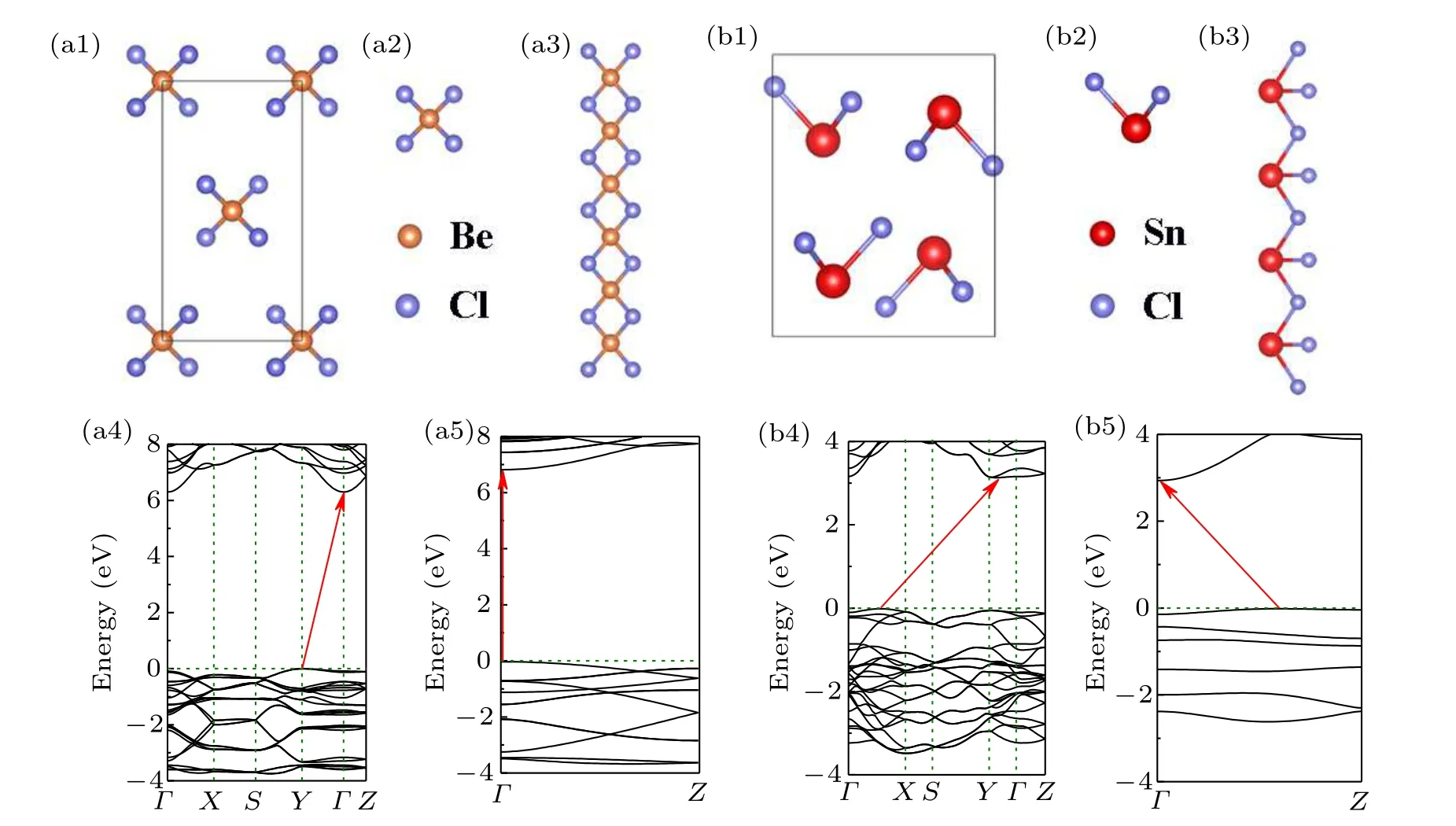
Fig.2. Crystal and electronic structures of two typical 1D vdW bulks and their 1D AWs. (a1)Side view of bulk BeCl2. (a2)Top and(a3)side views for 1D AW of BeCl2. The band structures of bulk BeCl2 (a4)and 1D AW of BeCl2 (a5). (b1)Side view of bulk SnCl2. (b2)Top and(b3)side views for 1D AW of SnCl2. The band structures of bulk SnCl2 (b4)and 1D AW of SnCl2 (b5).
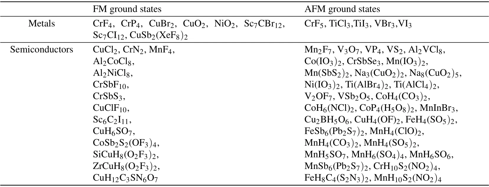
Table 2.Detailed list of 61 kinds of 1D magnetic AWs based on FM/AFM ground states and electrical properties of metal/semiconductors.Detailed magnetic and electronic properties are presented in Section VI of the SM.
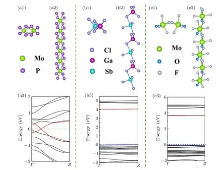
Fig. 3. Crystal and band structures of three representative 1D AW materials. (a1) Top and (a2) side views for 1D AW of MoP4. (a3) The band structures for 1D AW of MoP4. (b1)Top and(b2)side views for 1D AW of GaSbCl6. (b3)The band structures for 1D AW of GaSbCl6. (c1)Top and(c2)side views for 1D AW of MoOF4. (c3)The band structures for 1D AW of MoOF4.
Among the metallic 1D AWs,some behave like semimetals. As shown in Fig.3(a3),MoP4displays a linear dispersion character near Fermi level(EF). The similar linear dispersions are also present in 1D AWs of InI, NiO2, CuO2, TiI3, TcCl4,CrP4,Ta4SiTe4,CuSb2(XeF8)2,which are all listed in the SM.It implies the ultrafast carrier motilities and promising applications of these 1D AWs in high-speed electronic devices.[44,45]
In addition, the discovery of Mott insulators and superconductors in magic-angle graphene superlattices has stimulated extensive interest in the community to look for the systems with flat-bands structures.[46,47]From the theoretical results in SM,it is found that 123 kinds of 1D AWs demonstrate the flat-bands characters. Compared with the binary 1D AWs,the flat-bands prefer to occur in ternary and multi-element composed 1D AWs. For instance,the electron(hole)effective masses of 1D GaSbCl6and MoOF4are 132.7 m(14.5 m)and 77.4 m (26.5 m), respectively, where m is the mass of a free electron. The bandwidths of the conduction (valence) bands for 1D GaSbCl6and MoOF4are only 13.7 (28.5) meV and 23.4 (45.2) meV. The obvious difference between GaSbCl6in Fig. 3(b3) and MoOF4in Fig. 3(c3) originates from the valence band components near EF, which is completely contributed by Cl-3p orbitals in GaSbCl6and by the hybridized O-2p and F-2p orbitals in MoOF4. It also indicates that the flat bands show complex orbital dependencies in different 1D AWs. It is noted that the flat band physics here is nontrivial since the flat band occurs along the wire direction rather than the quantum confinement direction. Further considering the correlation effect between electrons in these flat bands systems,the 1D AWs may display various exotic quantum states, such as Hubbard insulators and superconductors.Thus, the flat-bands characters make these 1D AWs in particular the multi-element composed 1D AWs be ideal low dimensional systems to explore the correlated effect and exotic quantum phases.
4. Stability and exfoliation energy
Through analyzing the electronic structures, phonon spectra,and exfoliation energies of 1D AWs,the most promising and possibly synthesizable 1D AWs in experiments are proposed as follows. In terms of the thermodynamical stabilities and relatively lower exfoliation energies in SM,1D AWs of CuO2and MnF4are FM metal and FM semiconductor,respectively. Besides, 1D AWs of VBr3and VS2display AFM metal and AFM semiconductor characters,respectively.Moreover,1D AWs of TeBr2, SiCl2,and BeCl2demonstrate semiconducting properties with direct band gaps,which are in the range of ~0.66 eV–6.84 eV.Thus,these typical 1D AWs are highly expected to be prepared and applied in versatile electronic and optoelectronic devices with smaller scale. In this work, the undistorted 1D AWs have been systematically explored. In fact, due to the strong electronphonon coupling,these 1D AWs may undergo interesting Peierls distortions.For example, 1D carbon chain will form a dimerization configuration along the chain direction to minimize the total energy,resulting in the transition of 1D carbon chain from the metallic to insulating. For 1D AWs with more complex structures,the atoms would move and twist within 3D space,inducing more complex and interesting Peierls distortions. It is deserved to exploit in further work.
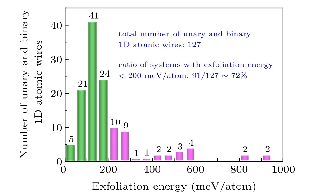
Fig. 4. Distribution of the exfoliation energies of unary and binary 1D AWs. The exfoliation energies of most 1D AWs are in the range of 50–200 meV/atom. The specific values of the exfoliation energies for all 1D AWs are listed in Table S1 in the SM.
5. Conclusion and perspectives
In this work,a database of 367 types of 1D AWs has been established,where the crystal structures,electronic properties,and stabilities are included based on DFT calculations. It is found that ~81% of 1D AWs are binary and ternary compounds. Furthermore, the unary and binary 1D AWs with relatively small exfoliation energy tend to be thermodynamically stable and 72% unary and binary 1D AWs are suitable to be mechanically exfoliated from their bulks. More significantly,the rich physical properties and quantum phases,such as 1D semiconductors,1D metals/semimetals,1D magnetism,shed light on potential applications of these 1D AWs in nextgeneration sub-nm electronic, spintronic, and energy relevant devices,etc. In addition,some 1D AWs possessing flat bands characters would provide an exciting and ideal platform to explore strongly correlated phenomena. Therefore,this database will offer a valuable resource for the scientific community to further explore 1D exotic quantum states and exploit practical 1D device applications based on 1D AW systems.
Acknowledgments
We are grateful for insightful suggestions and discussions from Dr. D.Y.Liu, Prof. L.J.Zou, and Dr. J.G.Geng. We also thank the computational resources and technical support from the National Supercomputer Center in Tianjin (TianHe-1 (A)) and the Supercomputing Center of Nankai University(NKSC).
杂志排行

Chinese Physics B的其它文章
- Corrosion behavior of high-level waste container materials Ti and Ti–Pd alloy under long-term gamma irradiation in Beishan groundwater*
- Degradation of β-Ga2O3 Schottky barrier diode under swift heavy ion irradiation*
- Influence of temperature and alloying elements on the threshold displacement energies in concentrated Ni–Fe–Cr alloys*
- Cathodic shift of onset potential on TiO2 nanorod arrays with significantly enhanced visible light photoactivity via nitrogen/cobalt co-implantation*
- Review on ionization and quenching mechanisms of Trichel pulse*
- Thermally induced band hybridization in bilayer-bilayer MoS2/WS2 heterostructure∗