Bio-organic Polymer Solar Cells Using DNA-CTMA: PSS as an Efficient Anode Buffer Layer
2021-04-22PANJingZHIPengweiJIAZheHUYi
PAN Jing,ZHI Pengwei,JIA Zhe,HU Yi
(Department of Materials and Chemical Engineering,Taiyuan University,Taiyuan 030032,China)
Abstract:Deoxyribonucleic acid (DNA)-cetyltrimethyl ammonium (CTMA) doped with poly(styrene-sulfonate) (PSS) is used to replace poly(3,4-ethylenediox-ythiophene)(PEDOT):PSS as a new bio-organic anode buffer layer. The all solution-processed solar cells with this new buffer are investigated in this paper. Compared to the reference cell employed PEDOT:PSS as anode buffer layer, the power conversion efficiency of the bio-organic photovoltaic cell is improved by 0.64%, which can be mainly attributed to the short circuit current density enhancement (by 9.20%). Significant increase of external quantum efficiency from 420 to 570 nm is obtained, consistent with the larger short circuit current. Besides the similar electronical performance, the inherently biodegradable and renewable features indicate DNA-CTMA:PSS as a promising alternative material to PEDOT:PSS as anode buffer layer for polymer solar cells.
Key words:Bio-Organic Polymer Solar Cell; DNA-CTMA:PSS; Anode Buffer Layer
1 INTRODUCTION
Because of the mechanical flexibility, portability and the potential of using roll-to-roll processing to produce low cost solar cells, polymer solar cells have been counted as a promising source of clean energy[1]. Most reported bulk heterojunction (BHJ) polymer solar cells (PSCs) comprise a phase separated mixture of interpenetrating networks of the conjugated polymers (electron donors) and fullerene derivatives (electron acceptors)[2,3]. Compared to the commercially produced solar cells based on silicon, the power conversion efficiency (PCE) of PSCs is much lower[4-6]. To improve PCE of the PSCs, many charge selective transport materials are designed and synthesized as buffer layers between electrodes and active layers[7-10]. Due to the proper energy levels and good optical properties, poly (3,4-ethylenediox-ythiophene):poly (styrene-sulfonate) (PEDOT:PSS) is the most common used anode buffer layer between indium tin oxide (ITO) and active layers.[11-12]
Using buffer layer of PEDOT:PSS can not only improve the surface quality of ITO, but also lead to significant improvement of external quantum efficiency of PSCs due to its hole transporting and electron blocking ability[13]. However, the relatively high acidity of PEDOT:PSS tends to corrode ITO and degrade PSCs performances[14]. Other disadvantages of PEDOT:PSS being anode buffer layer, such as inhomogeneous film morphologies, electrical inhomogeneity and poor electron blocking capacity were also reported[15, 16]. To avoid these problems, new buffer materials have been designed to replace PEDOT:PSS and some showed improved performance over those using PEDOT:PSS buffer layer[17-19]. Compared to those synthetic compounds, deoxyribonucleic acid (DNA) possesses unusual optical and electronical properties due to its unique double helix structure. Derived from the waste of the salmon fishing industry, DNA is abundant, affordable and renewable[20]. It is also environment-friendly and inherently biodegradable. Preliminary researches show that the band-gap of DNA complex is over 4 eV and the lowest unoccupied molecular orbital level is 0.9 eV, which suggest that DNA can be promising alternative buffer layer of PEDOT:PSS[21]. However, DNA complex is soluble only in aqueous solutions, which is not compatible with typical fabrication process of PSCs. By an ion exchange reaction with cetyltrimethyl ammonium (CTMA), DNA-CTMA complex would be water-insoluble and soluble in many of the alcohols. Furthermore, the DNA-CTMA film is thermally stable up to 200~250 ℃ and can be used in the fabrication of PSCs[20]. Though DNA-CTMA complex is supposed as suitable anode buffer layer, the open circuit voltage (Voc) of PSCs using pure DNA-CTMA complex is only 200 mV, much lower than those with PEDOT:PSS buffer layers[22]. One of the main reasons for this low Vocis the relatively low conductivity of DNA-CTMA thin films[23]. To overcome this shortcoming, anamphiphilic surface active agent, PSS can be used to improve the electronic conductivity of DNA-CTMA.
In this paper, a layer of DNA-CTMA nanowires doped with PSS (DNA-CTMA:PSS) is coated on top of ITO by an all-solution processing approach. With this novel bio-organic DNA-CTMA:PSS buffer layer, PSCs of similar performances to those with PEDOT:PSS anode buffer layer are obtained.
2 EXPERIMENTS
The solution of DNA-CTMA nanowires were prepared by an all-solution processing method. The double-helix salmon DNA with molecular weight of 3.3×10⁴g/mol (mean molecular length of 50 bp) bought from Sigma Aldrich is aqueous soluble only. Ion exchange reactions between DNA and CTMA with molecular weight of 319.20 g/molpurchased also from Sigma Aldrich were used to produce DNA-CTMA, which is aqueous insoluble but soluble in ethanol and butanol. Equal mass fraction of DNA and CTMA (1g) were dissolved in 500 ml of distilled water, respectively. To make DNA and CTMA dissolved completely, both solution were magnetic stirred under room temperature slowly for 8 hours to form clear solution. After dissolution, the DNA solution was dropwise added into the CTMA solution slowly and the mixture of two solutions was magnetic stirred when the DNA solution was added. The DNA-CTMA precipitates were collected by centrifugal separation: 6 centrifugal tubes each contains 30 ml suspension of DNA-CTMA werecentrifuged at 8000 r/min for 180 s. Then the DNA-CTMA precipitates wereultrasonic washed by extra distilled water for 20 min (5 times) to get rid of Na ion. And then, the product was vacuum dried at 40 ℃ for 10 h to obtain DNA-CTMA nanowires. Finally, the DNA-CTMA nanowires were collected in ground glass stoppered bottles for further usage.
To prepare DNA-CTMA:PSS buffer layer, the DNA-CTMA nanowires were first dissolved in n-butanol (99.0% mass fraction) to form DNA-CTMA butanol solution with concentration of 20 mg/ml; this solution was magnetic stirred at 60 ℃ for 4~6 h. A certain amount of PSS were dispersed in n-butanol solution to form solutions of 0.4, 0.2, 0.1, 0.05 and 0.01 mg/ml for further usage. Then, equal volume of DNA-CTMA and PSS solution were mixed to prepare DNA-CTMA:PSS solution. The structure of the proposed bio-organic PSCs with DNA-CTMA:PSS buffer layer is shown in figure 1. DNA-CTMA:PSS solution was spin-coated on top of a cleaned ITO patterned glass substrate at 800 r/min for 60 seconds. P3HT (Aldrich) blended with PCBM (Aldrich) was dissolved in chlorobenzene (10 mg/ml) and spin-coated onto the DNA-CTMA:PSS nanowire layer at 800 r/min for 20 s. The solvent annealing was carried out under chlorobenzene atmosphere for 30 min. Then, these devices were transferred into a vacuum environment(5×10⁻⁴Pa) for thermal deposition of aluminum electrodes (100 nm). When the solar cell devices were fabricated, thermal annealing was carried out in vacuum at 150℃ for 30 min. The current-voltage (I-V) characteristics of these devices were measured by a Keithley 2400 source meter under 100 mW/cm2AM1.5G illumination (Newport). All fabrication and measurement processes were performed at room temperature. Also, PSCs with buffer layer of PEDOT:PSS and DNA-CTMAwere fabricated as reference devices.
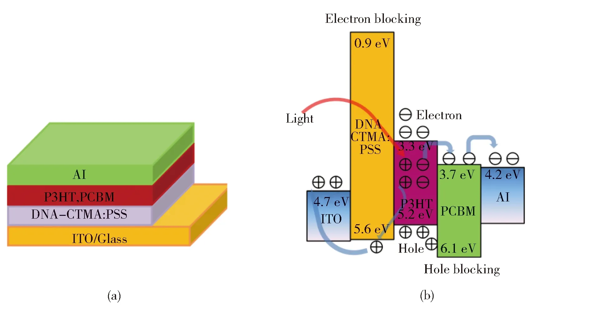
Fig.1 (a) Schematic device structure of bio-organic PSC which employs DNA-CTMA:PSS as buffer layer.and (b) The energy level diagram
3 Results and discussion
3.1 Device performance
Besides finishing rough surface between ITO and the active layer, DNA-CTMA:PSS buffer layers mainly serve as hole extraction layer as well as electron blocking layer. The proposed bio-organic PSCs is designed as ITO/DNA-CTMA:PSS/P3HT:PCBM/Al (figure 1). With the lowest unoccupied molecular orbital level (0.9 eV), the bio-organic buffer layer DNA-CTMA could block electron from wrong direction much more efficiently. However, the barrier between the HOMO of DNA-CTMA and the active layer might stunt the transfer process of holes, which may degrade performance of the proposed PSCs.
The J-V characteristics of three PSC devices with different buffer layer are shown in figure 2 and theextracted photovoltaic parameters are shown in table 1. As shown in table 1, the PCE of PSC with buffer layer of DNA-CTMA:PSS is improved by 119.58%, compared to PSC with buffer layer of DNA-CTMA; TheVocis improved by 27.08% and the short-circuit current (Jsc) is improved by 105.78%. This suggests that the enhancement of PSCs using buffer layer of DNA-CTMA:PSS is mainly driven by the increase of Jsc. It also means that doping PSS in DNA-CTMA complex would improve the electron conductivity of DNA-CTMA film significantly. Experimental results show that electron conductivity of DNA-CTMA:PSS (0.1 mg/ml) film is 2.12×10⁻³Ω-1·m-1, which is much higher than that without doping of PSS (6.70×10⁻⁵Ω-1·m-1). PCE of the proposed bio-organic PSCs is almost the same as that with buffer layer of PEDOT:PSS. They also have similarVocand fill factor (FF) to the reference device with PEDOT:PSS buffer layer. While, theJscincreases by 9.20% compared to that with PEDOT:PSS buffer layer. Compared to the band gap of the reference buffer layer of PEDOT:PSS (about 1.7 eV), the band gap of DNA-CTMA (about 4.7 eV) is much higher, which means it might provide higher transmittance and allow more photons to be absorbed by the active layer. However, as shown in figure 3, the two buffers show almost the same transmittance to let the same amount of photons to be absorbed by the active layer. Similar PCE of devices with buffer layer of PEDOT:PSS and DNA-CTMA:PSS suggests that DNA-CTMA:PSS is a promising alternative of PEDOT:PSS. However,Vocof PSCs with buffer layer of DNA-CTMA decreases by 6.10% than that with buffer layer of PEDOT:PSS.
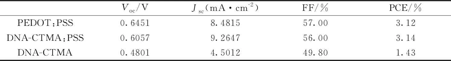
Table 1 The photovoltaic parameters of cell devices with different buffer layers (I).

Fig.2 The illuminated current-voltage characteristics of PSCs with buffer layer consists of PEDOT:PSS, DNA-CTMA, DNA-CTMA:PSS. All J-V characteristics are measured under AM 1.5G illumination.

Fig.3 Photo-absorption of the buffer layer of PEDOT:PSS and DNA-CTMA:PSS.
The light absorption of the devices with buffer layers of PEDOT:PSS and DNA-CTMA:PSS are shown in figure 4 and the external quantum efficiency (EQE) of these devices are shown in figure 5. Compared to the conventional PSC which uses PEDOT:PSS as buffer layer, light absorption of the proposed bio-organic PSC from 300 to 600 nm is slightly higher than that of the conventional device. Also can be in figure 5, the EQE of this proposed bio-organic PSC around 500 nm is higher than the device with buffer in layer of PEDOT:PSS.
To study the hole transport properties of different buffer layers, impedance spectra are measured and shown in figure 6. Each impedance spectra appear to be a semicircle and can be fitted by the equivalent circuit. The parameters including series resistance (Rs), parallel resistance (Rp), capacitance (C) and relaxation time of the devicesare are shown in table 2. It is shown thatRsand capacitance of the PSCs with three different buffer layers remain almost the same to each other. However,Rpof the proposed device with DNA-CTMA:PSS buffer layer decreases significantly. Compared to devices with buffer layers of DNA-CTMA and PEDOT:PSS, it decreases by 42.29% and 35.41%, respectively. This can be assigned to the inhomogeneity of doping PSS in DNA-CTMA which might increase the leakage current. Also, PSC with DNA-CTMA:PSS has the shortest relaxation time, which suggests the doping of PSS in DNA-CTMA can enhance device stability.

Table 2 The photovoltaic parameters of cell devices with different buffer layers (II).
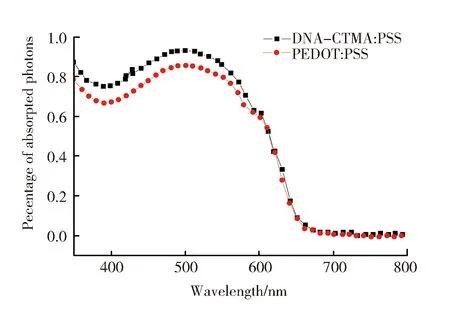
Fig.4 The absorption of the devices with buffer layers of PEDOT:PSS and DNA-CTMA:PSS.

Fig.5 EQE spectra of devices with buffer layer of PEDOT:PSS only,DNA-CDMA nanowire only,and the proposed bio-organic buffer layer

Fig.6 Nyquist plots of the EIS of DNA-CTMA, DNA-CTMA:PSS and PEDOT:PSS buffer layers.
3.2 Microstructure of the bio-organic buffer layer
Scanning electron microscopy (SEM) images and transmission electron microscope (TEM) images of this proposed bio-organic DNA-CTMA:PSS are shown in figure 7 and figure 8, respectively. SEM images show that the DNA-CTMA nanowires are dispersed homogeneously. This property results in great transmittance over spectrum of UV and visible light, which will enhance the generation of photocurrent[24]. Comparison of surface roughness between ITO coated by DNA-CTMA:PSS buffer layer (figure 9(a)) and uncovered ITO (figure 9(b)) shows that this biological buffer layer can reduce surface roughness of ITO, which results in the improvement of performance of polymer photovoltaic cells.

Fig.7 SEM image of DNA-CTMA:PSS layer on ITO.

Fig.8 TEM image of DNA-CTMA:PSS.
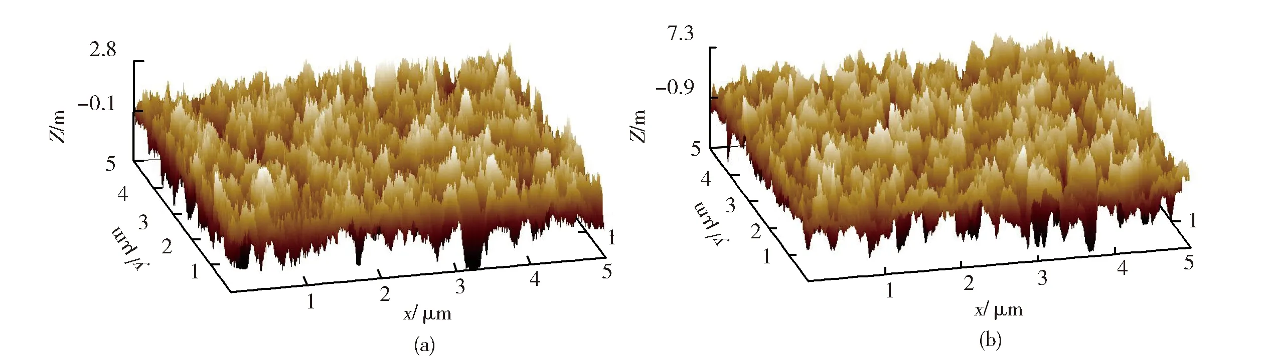
Fig.9 Surface roughness of (a) DNA-CTMA:PSS coated on ITO and (b) uncovered ITO.
3.3 Impact of PSS doping concentration on device performance
It is shown that doping PSS in DNA-CTMA would enhance the conductivity of DNA-CTMA film significantly, leading to the improvement of PSCs. Because of the electrical insulation of PSS, excess amount of PSS would degrade the conductivity of DNA-CTMA film. To find the optimal doping ratio, six types of PSCs were designed with different blend ratios. Their performance are shown in figure 10 and listed in table 3. It is shown that PSCs with buffer layer of DNA-CTMA blended with PSS (0.1 mg/ml) perform best among these devices. However, the reason that doping the isolative PSS into DNA-CTMA can improve film conductivity is not clear now.
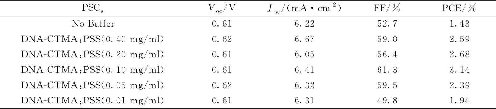
Table 3 The photovoltaic parameters of cell devices with DNA-CTMA:PSS layers of different doping ratios.

Fig.10 The illuminated current-voltage characteristics of PSCs with DNA-CTMA:PSS buffer layer with different PSS blend rations.
4 Conclusion
In this work, bio-organic PSCs which used DNA-CTMA:PSS as buffer layer are fabricated. Compared to the PSCs with PEDOT:PSS buffer layer, the proposed bio-organic PSCs show similar device performance. Due to its unique optical and electric properties, DNA-CTMA:PSS show great potentials to replace PEDOT:PSS to be a new promising anode buffer material. And the use of DNA-CTMA:PSS will reduce the fabricating cost of PSCs and make it environment friendly.
