In-situ reduction of silver by surface DBD plasma:a novel method for preparing highly effective electromagnetic interference shielding Ag/PET
2021-03-22ZhiyuanFAN范志远LanboDI底兰波DecaiBU部德才TengdaZHANG张腾达andXiulingZHANG张秀玲
Zhiyuan FAN (范志远), Lanbo DI (底兰波), Decai BU (部德才),Tengda ZHANG (张腾达) and Xiuling ZHANG (张秀玲)
College of Physical Science and Technology, Dalian University, Dalian 116622, People’s Republic of China
Abstract Electromagnetic interference (EMI) shielding composites with good flexibility and weatherability properties have attracted increased attention.In this study, we combined the surface modification method of sub-atmospheric pressure glow discharge plasma with in situ atmospheric pressure surface dielectric barrier discharge plasma(APSDBD)reduction to prepare polyethylene terephthalate supported silver (Ag/PET).Due to the prominent surface modification of PET film,mild plasma reduction,and effective control of the silver morphology by polyvinylpyrrolidone (PVP), a 3.32 μm thick silver film with ultralow sliver loading(0.022 wt%)exhibited an EMI shielding efficiency(SE)of 39.45 dB at 0.01 GHz and 31.56 dB at 1.0 GHz (>30 dB in the range of 0.01-1.0 GHz).The SEM results and EMI shielding analysis indicated that the high performance originated from the synergistic effect of the formation of silver nanoparticles (AgNPs) with preferentially oriented cell-like surface morphologies and layer-by-layer-like superimposed microstructures inside, which demonstrated strong microwave reflection properties.Fourier transform infrared spectrometer and x-ray diffractometer showed that the surface structures of the heat-sensitive substrate materials were not destroyed by plasma.Additionally, APSDBD technology for preparing Ag/PET had no special requirements on the thickness, dielectric constant, and conductivity of the substrate, which provides an effective strategy for manufacturing metal or alloy films on surfaces of heat-sensitive materials at a relatively low cost.
Keywords: Ag/PET, atmospheric pressure cold plasma, surface dielectric barrier discharge,polyvinylpyrrolidone, electromagnetic interference shielding
1.Introduction
Electronic instruments, which use electrical energy for transmission and signal distribution, such as in radio receivers, telephone communications, automotive electronics, and cables,can generate electromagnetic radiation.Electromagnetic radiation can not only affect the electrical and magnetic conductivity of electronic devices but also influence the surrounding environment, directly threatening human health.Therefore,effective electromagnetic interference(EMI)shielding materials have attracted much attention [1-3].
Traditional EMI shielding materials mainly include magnetic oxides [4, 5], carbides [6, 7], and metal-based materials [8-10].Magnetic oxides have excellent magnetic conductivity energies.However, they have difficulty meeting the effective shielding requirements of electronic devices[11,12]and supercapacitors[13,14]in terms of thinning and flexibility, which has become a key factor restricting their development.Carbides,especially carbon nanotubes[15-17],carbon fiber fabrics[18,19],graphene[20, 21],and the likes in combination with magnetic constituents [22-24], have attracted much attention recently.With good flexibilities and porous and loose structures, the conductive filling materials can be controlled and adjusted to utilize interlayer structures to enhance the reflected and absorbed electromagnetic radiation[16, 18, 21].In spite of this, when it comes to achieving the required performance,further breakthroughs are required.Furthermore, due to the high resistivity in the transmission process, porous materials will affect the conductive magnetic conductivity energy, thus, relative debugging methods are strongly needed[17,23,25].Metal-based shielding materials have superb conductivities, making them the first choice for effective EMI shielding materials.Nevertheless, their high densities,low environmental stabilities,weak flexibilities,and manufacturing challenges limit their applications in flexible electronics, spacecraft, and automobiles [8, 10].Meanwhile,common traditional EMI shielding material preparation technologies mainly use thermal spraying [26], sputtering[27], pulsed laser deposition [28], chemical vapor deposition[29], electroplating [30], electroless plating [31], and laser induction [32], but these methods must be equipped with large-scale devices.Additionally,a large number of chemical reagents have to be introduced for some methods,which may increase the number of uncontrollable factors in the experiment, endangering the health of workers as well.
Researchers have developed relatively safe preparation methods, with low dependencies on high-precision equipment.Meanwhile,a new scheme using EMI materials that are lightweight with high conductivities and adhesion properties has been proposed: adding conductive fillers to the polymer matrix [33, 34].Based on the flexibility of the polymers,admirable weatherability performances, and ease of processing and manufacturing, the types and additional conditions of the fillers can be selectively regulated and controlled to meet the needs of an application,and thus,the preparation of the most economical, efficient, and high-performance reprocessing composite material can be realized.The feasibility of the scheme focuses on the selection of the polymer matrix and conductive filler.In recent years, new polymer flexible materials, with excellent optical transparencies, weather resistances, chemical stabilities, high hygroscopicities, weak acid resistances,organic solvent resistances,friction and wear resistances, creep resistances, fatigue resistances, and other properties, have been widely applied in flexible device substrate materials [35, 36].Among these materials, due to the superior toughness properties of thermoplastics, polyethylene terephthalate (PET) has been regarded as a top choice for flexible polymer substrate materials [37].For conductive fillers, nickel, cobalt, copper, and silver are all ideal choices.Compared with other materials,silver has a high conductivity(6.8 × 10⁵S cm−1), predominant oxidation resistance, low corrosion resistance,and inexpensive production cost,making it the best filler for preparing highly conductive composite materials [23, 38].
Hu et al[39]proposed a high-yield strategy for preparing silver nanowires by injecting polyol in two steps.PES/silver nanowire/PET films with good stabilities,conductivities,and light transmittance properties were prepared, and the corresponding EMI shielding effectiveness (SE) was 38 dB.Yamada et al [40] reported a new printing technology that could replace the traditional vacuum and lithography equipment processing.The unique chemisorption phenomenon was used to weakly encapsulate silver nanoparticles (AgNPs),triggering the self-fusion of high-resolution patterned silver layers to the substrate to form sub-micron fineness silver patterns.Yang et al [41] presented a mechanical-chemical coupling method to fabricate independent conductive thin films with unstable-driven layered micro/nanostructured modes.This strategy greatly expanded the application field of wrinkle technology and provided ideas for the design of advanced thin-film materials and corresponding devices.Jia et al [42] used a simple and low-cost Mayer-rod coating method to fabricate an efficient transparent EMI shielding film composed of calcium alginate (CA), silver nanowires(AgNWs), and polyurethane (PU).The EMI SE performance of the high transmittance CA/AgNW/PU film reached 20.7 dB, meeting the demands of commercial shielding applications.Oh et al[43]recently demonstrated a dry plasma reduction process for the effective synthesis and immobilization of metal nanoparticles on PET films at atmospheric pressure and near room temperature.When the precursor solution concentration reached 500 mM, the reduced silver layer exhibited an EMI SE value as high as 60.49 dB,exceeding the previously reported EMI shielding maximum index.To solve the problem of Ag nanoparticles aggregation,they further added seed metals such as Ag, Cu, Fe and Ni before preparing the Ag layer [44].Uniform Ag layer was successfully fabricated on the metal seed-PET substrate, and the Ag layer formed on the surface of Bi seed/PET substrate showed relatively high EMI shielding efficiencies.
At present,studies have mainly focused on the regulation of the interlayer structures and surface interface morphologies of highly conductive EMI shielding materials [3, 16,27,45].Effective shielding is achieved through the following three mechanisms.First, carriers are effectively generated by the interactions between the shielding materials and electromagnetic fields to reflect radiation.Second, electromagnetic characteristics or interactions between magnetic dipoles and radiation are used to promote the absorption of electromagnetic radiation.Third, multiple internal reflections arise from scattering centers, interfaces, or defect points inside the shielding material to improve the electromagnetic shielding effect [4, 19, 20, 46].
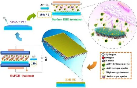
Figure 1.Schematic diagram of the Ag/PET film preparation process.
In this study,using no added chemical reduction reagents,a silver nitrate solution was dripped on a modified PET film surface and reduced in situ to prepare silver films via the safe and simple atmospheric pressure surface dielectric barrier discharge plasma(APSDBD)method.A 3.32 μm thick silver film exhibited EMI SE of 39.45 dB at 0.01 GHz and 31.56 dB at 1.0 GHz, which were >30 dB in the range of 0.01-1.0 GHz.The high EMI SE at an ultralow sliver loading (0.022 wt%)resulted from both the formation of surface preferentially oriented cell-like-morphology AgNPs and a layer-by-layer-like superimposed microstructure inside, which showed that reflection is the dominating shielding mechanism.APSDBD technology for preparing Ag/PET has no special requirements on the thickness, dielectric constant, and conductivity of the substrate, providing a new idea for surface functionalization preparation of heat-sensitive materials.The obtained Ag/PET exhibited excellent performances, and thus it has potential applications in the field of portable and wearable intelligent EMI electronic products.
2.Experimental
Silver nitrate (AgNO3) and polyvinylpyrrolidone (PVP,molecular weight ≈1300 000) were purchased from Komeito Chemical Reagents Co.,Ltd(Tianjin,China).The viscosity of 10.0 g·l−1PVP solution was determined using Ostwald viscosimeter, which was 1.138 × 10⁻³Pa·s at 25 °C.PET film(thickness: 0.2 cm) was obtained from Fuyuanda Plastic Manufacturing Co., Ltd (Guangdong, China) and cut into 4.0 cm × 4.0 cm size for later use.Anhydrous ethanol was obtained from Komeito Chemical Reagents Co.,Ltd(Tianjin,China).
2.1.PET film surface treatment and preparation of Ag/PET samples
All experiments were carried out on a PET film substrate with a size of 4.0 cm × 4.0 cm × 0.2 cm.Before cold plasma treatment, PET film was immersed in ethanol, washed with deionized water,placed on a culture dish(sterilized),and dried at room temperature in a vacuum drying device for later use.
Figure 1 shows a flow diagram of the Ag/PET film preparation process.The whole process can be divided into two steps: sub-atmospheric pressure glow discharge plasma(SAPGD) surface modification treatment of PET film and APSDBD reduction preparation of Ag/PET samples.
Modification of PET film surface: SAPGD was used to treat the PET film substrate surface.Cold plasma surface modification was performed using a HPD-280 SAPGD surface treatment system produced by Nanjing Suman Electronics Co.,Ltd(Nanjing,China)[47].The chamber consisted of parallel plate electrodes with a spacing of 32.0 cm, a discharge frequency of 20 kHz, an air pressure of 2.0 × 10³Pa,and a discharge time of 180 s.The water contact angle of the PET film has been decreased from 60.0° to 17.5° after SAPGD treatment (figure S1, available online at stacks.iop.org/PST/23/035502/mmedia).

Figure 2.Digital photographs of (a) pristine PET, (b) Ag/PET-1,(c) Ag/PET-2, (d) Ag/PET-5 and (e) Ag/PET-10.
Preparation of Ag/PET samples: PET film was immediately placed in the APSDBD chamber [48] after surface modification treatment, and the precursor solution was quantitatively (100 μl) dropped onto the modified PET film surface using a pipette gun.APSDBD electrode system consisted of a comb-like discharge electrode and an induction electrode made of tungsten.The APSDBD was powered by an AC power supply composed of a DPO 2014 Function Generator, an FL1200 single-phase electric parameter tester,and a CTP-2000K plasma generator.The driving AC frequency of 10.4 kHz was amplitude-modulated to produce sine waves, and the relative peak-to-peak sinusoidal high voltage was adjusted to 5.8 kV.The chamber was equipped with gas feed input/output ports and a high-voltage interface.A mixture of high-purity argon and hydrogen(>99.999%)was used as the working gas.The total flow rate of the working gas was 100 ml·min−1, with a ratio of argon to hydrogen of 1:1.Ag/PET samples were placed 6 mm below the surface dielectric barrier discharge (DBD) electrode to reduce the inhomogeneity of the samples caused by the comb-like discharge reduction, and one sample was discharged three times for 3 min each time to avoid the agglomeration of AgNPs caused by thermal treatment [48].After surface DBD cold plasma reduction treatment, Ag/PET samples were dried in the vacuum drying oven at 80 °C for 3 h in the dark.Moreover,Ag/PET samples were marked as Ag/PET-1, Ag/PET-2,Ag/PET-5, and Ag/PET-10 based on the silver loading concentrations (1.0, 2.0, 5.0, and 10.0 mM·l−1) of the precursor solution (homogeneous solution of AgNO3and polyvinylpyrrolidone (PVP)).The concentrations of PVP (1.0,2.0, 5.0, and 10.0 g·l−1) were mixed to silver loading concentrations (1.0, 2.0, 5.0, and 10.0 mM·l−1, respectively).
2.2.Characterization
X-ray diffractometer (XRD, DX-2700) was used to characterize the Ag/PET samples with Cu-Kα1ray(λ = 1.541 78 Å).The valence state of elements in the silver film obtained by reduction was understood by Kαx-ray photoelectron spectrometer (XPS, Thermo, ESCALAB-250)and the calibration was carried out concerning C1s peak with the energy of 284.6 eV.The functional group changes on the silver film surface were performed by Fourier transform infrared spectrometer (FTIR, Thermo, Nicolai 6700), attenuated total reflection (ATR, PIKE technology) in the range of 4000-400 cm−1was set, with a resolution of 4 cm−1and 32 scans accumulated.The scanning electron microscope(SEM, Zeiss, Sigma 500) was adopted to test the surface morphology of the sample at an accelerated voltage of 5 kV,and the scanning electron microscope images were taken at a magnification of 10 000, 20 000 and 50 000 times.
Using a microwave vector network analyzer (Agilent N5230C), the EMI shielding indices of the silver films were obtained in the frequency range of 0.01-1.0 GHz through the coaxial transmission line method,and the corresponding EMI SE was evaluated as well.
3.Results and discussion
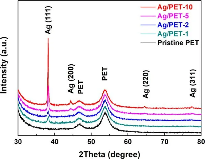
Figure 3.XRD patterns of pristine sample, Ag/PET-1, Ag/PET-2,Ag/PET-5 and Ag/PET-10.
The apparent morphologies of the Ag/PET samples prepared by reduction, loaded with different precursor concentrations,were photographed via a digital camera, as illustrated in figure 2.The surface of the pristine PET film was colorless.Compared with the pristine PET film, the obtained Ag/PET sample surfaces exhibited a bright silver color, which gradually deepened with the increase in the concentration of the loaded precursor solution, and the corresponding light reflectivity also changed accordingly.The Ag/PET-10 sample exhibited an evident Torrance reaction (silver mirror reaction), revealing that based on the modified surface of the PET film, the effective assistance of the capping agent PVP,and the cooperative preparation method of APSDBD reduction, silver ions were successfully reduced into AgNPs and closely arranged to form silver films [4, 28, 31].Meanwhile,the silver loading on PET surface were roughly calculated as 0.011, 0.022, 0.054 and 0.110 wt%, corresponding to Ag/PET-1, Ag/PET-2, Ag/PET-5 and Ag/PET-10.With the increase in the Ag ion concentration, the thickness of silver films increased,which deepened the colors of the samples and enhanced the reflectivity[49,50].Furthermore,there are also some several advantages:it is simple(two steps),fast(several minutes), and green (no addition of other environmentally unfriendly chemicals).
To understand the physical and chemical processes of silver ion conversion to AgNPs, XRD and XPS assessments were employed.The crystal forms and phase structures of the samples were identified by XRD characterization and analysis.As shown in figure 3, the pristine PET film sample exhibited two characteristic peaks, located at 46.77° and 53.76°.However, for the Ag/PET samples, sharp silver characteristic peaks appeared at 38.22°, 44.37°, 64.59°, and 77.55°, corresponding to the (111), (200), (220), and (311)crystal planes,respectively(JCPDS card,file no.65-2871),of the silver face-centered-cubic structure [47, 51].Meanwhile,the preferred orientation of the(111)crystal plane occurred in the XRD patterns, and the intensities of the characteristic peaks increased with increasing precursor concentration.This indicated that the AgNPs could be effectively formed by in situ reduction.Meanwhile, under the strong morphology control of the capping agent (PVP), the free energy of each surface of the silver face-centered cubic polyhedron increased in the order of {111} < {100} < {110}, which caused the AgNPs to arrange in the most stable morphology(at low free energy), significantly changing the growth trend of the silver crystal surface [31, 52, 53].No characteristic diffraction peaks of AgNO3were detected in the obtained XRD pattern results, which means that silver ions may have been completely reduced to AgNPs.This explains why no AgxO peaks were found in the XRD patterns.This can be confirmed from the XPS spectra (figure 4) as well.
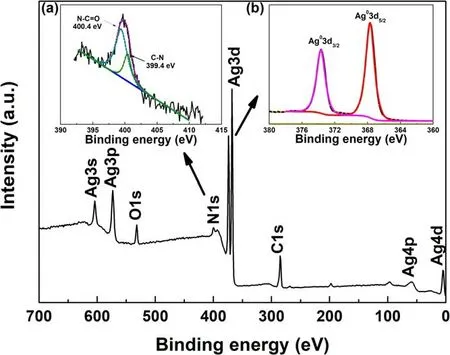
Figure 4.XPS survey spectrum of Ag/PET-2 sample and inset:XPS spectra of (a) N1s and (b) Ag3d.
The element types and corresponding valence states of the silver films formed on the PET film surface were further confirmed.Figure 4 presents the full spectrum of the Ag/PET-2 film.Peaks of oxygen and silver were evident.The oxygen mainly corresponded to the C=O bond in the PVP structure (figure S2).Meanwhile, combined with the fitting result of the C1s spectrum(figure S3),corresponding oxygencontaining groups(N-C=O and C=O)were present[54,55].Moreover, C-N bond in 2-pyrrolidone aroused by PVP dissociation (figure S2) was measured as well (figure S3).The inset(figure 4(a))shows the N1s XPS spectrum,which can be deconvoluted into two peaks at 400.4 and 399.4 eV, respectively, corresponding to the N-C=O and C-N bonds originated from PVP.Meanwhile, no characteristic NO3−peaks were evident, which confirmed the complete reduction of the AgNO3.The N-C=O and C-N bonds originated from PVP are also verified by the following FTIR results (figure 5).To further verify the reduction capability of the surface DBD cold plasma and evaluate the purity of the AgNPs obtained by reduction treatment, the Ag3d XPS spectrum was fitted.As shown in the inset (figure 4(b)), the composition of metallic silver in the Ag/PET-2 sample was as high as 100%, which demonstrated that the surface DBD plasma had a high-efficiency reduction capability [48].
To understand the chemical changes of the PET film surface after cold plasma treatment, FTIR was used to detect the changes in chemistry that occurred on the surface of the PET film.The infrared spectra of the pristine PET film sample, the surface-modified PET film sample, and the Ag/PET samples with different precursor concentrations are shown in figure 5(a).Several characteristic peaks are evident in the spectrogram.However, the overall trends of several samples were consistent, and no new peaks appeared.Due to the non-thermodynamic equilibrium characteristics of the cold plasma, the surface structures of the flexible substrates were not changed [48, 56, 57].
PET compounds can be easily distinguished by the C=O,C-O, and C-H bonds of the ketone, aliphatic, and aromatic groups in the ranges of 1740-1670, 1090-1025, 1050-1030,and 900-700 cm−1, as reported by Ioakeimidis et al [58].As shown in figure 5(a), in the range of 3700-3400 cm−1, two strong peaks and one weak peak were exhibited.The weak peak at 3632 cm−1was attributed to the O-H bond of water.The strong peaks at 3548 and 3432 cm−1can be interpreted as alcohol groups and hydrogen bonds of the PET, the characteristics peaks of which can be detected at 1460 and 978 cm−1as well.Meanwhile,three peaks were evident in the range of 3080-2900 cm−1.The peak at 3066 cm−1was considered to be due to the C-H stretching vibration mode on the benzene ring, which also appeared at 1965 and 1580 cm−1.Furthermore, the peak at 2968 cm−1was the methyl (CH3)asymmetric stretching vibration.Similarly,peaks due to these vibrations are evident at 1460 and 1360 cm−1.The peak at 2900 cm−1corresponded to methylene (CH2) asymmetric tensile vibrations, and the corresponding peak at 856 cm−1corresponded to methylene rocking vibration [59].Focusing on figure 5(b), the C=O tensile vibrations appeared in the region from 2000 to 1500 cm−1, and the broad absorption band appeared in the region of 1740-1684 cm−1corresponded to C=O of both the aliphatic and carboxylic acid groups.C-O appeared in the fingerprint region,which ranged from 1400 cm−1to 1000 cm−1.Also, as illustrated in figure 5(c),the peaks appearing at 1088 and 1030 cm−1were the C-O stretching modes, which may have been related to the broad absorption band of C=O, involving different structures of aliphatic and carboxylic acid groups.Moreover,the in-plane and out-of-plane telescopic vibrations of the C=O bond appeared at 750-700 cm−1, in which the bond is evident at 730 cm−1in figure 5(c) [60, 61].
The comparative analysis of the pristine and modified samples showed that the strengths of the three bonds C=O(figure 5(b)), C-O (figure 5(c)), and O-H (figure 5(c))increased after SAPGD treatment.Due to the collision energy transfer mechanism of high-energy electrons, unstable substances in the PET were excited to separate from the polymer chain,reacting with reactive oxygen species(O,O*,and O2*)generated by cold plasma to form carboxylic acid (COOH)and lipid groups on the PET surface [61-63], resulting in changes of the hydrophilicity (figure S1) [64].However,compared with the modified sample,the strength of the C=O(figure 5(b)), C-O (figure 5(c)), and O-H (figure 5(c)) of the Ag/PET sample exceeded the effect of the SAPGD treatment.Meanwhile,the absorption bands of C=O and C-N stretching vibrations shift from 1664 to 1284 cm−1for pure PVP(figure 5(d)) to 1738 and 1345 cm−1(figures 5(b), (c)),respectively, corresponding to the N-C=O and C-N stretching vibrations.These are consistent with the XPS results,which may be induced by the dissociation of the PVP during cold plasma treatment.They can wrap and interact with the silver species by the N-C=O functional groups.Therefore, they are beneficial to stabilize the AgNPs and make them grow along a specific crystal plane.
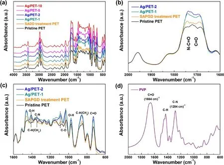
Figure 5.(a) FTIR of pristine sample, Ag/PET-1, Ag/PET-2, Ag/PET-5, and Ag/PET-10 in the range of 4000-400 cm−1, (b) changes in peak intensity of C=O bond(1762-1670 cm−1)in the infrared spectra,(c)changes in peak intensities of C-N bonds(1350-1340 cm−1),C-O bonds (1112-1020 cm−1), and O-H bonds (1412-1406 cm−1, 990-970 cm−1) in the infrared spectrum, and (d) FTIR spectrum of pure PVP.
Under the activation of the active species produced by the cold plasma, many residual active ions and metastable particles could continue to react to form corresponding functional groups, which was proven by the XPS analysis once again(figure S3)[54,55,63].In addition,the increase in the number of C-H bonds at 1460,1408,and 1360 cm−1was interpreted as the metastable substance (CH2) from the dissociation of PVP on the PET film surface being activated to react with gas particles(H2)under the energy transfer of highenergy electrons generated by the cold plasma, forming a stable substance (CH3) in the polymer chain [63-65].
To determine the arrangement of the AgNPs on the PET film surface,SEM analysis was carried out,and SEM images of the Ag/PET-1 and Ag/PET-2 were obtained.The crosssectional images of the samples were also obtained.As shown in figures 6(a)-(c),compared with the pristine sample surface,the Ag/PET surface exhibited morphological changes.Meanwhile, the change of the silver precursor concentration mainly resulted in the change of the particle sizes (DAg),which were ca.30.3 ± 20.3 and 43.6 ± 23.3 nm, respectively, for Ag/PET-1 and Ag/PET-2 (figures 6(b) and (c)inset)[32],corresponding to the DAgvalues of the Ag/PET-1(ca.26.7 nm)and Ag/PET-2(ca.37.2 nm)samples calculated from the Ag (111) peak in the XRD patterns (figure 3)[31,52,53].Due to the presence of the capping agent(PVP),the AgNPs formed a compact cell-like microstructure on the PET film surface, which was related to the preferred orientation of the Ag (111) in the XRD patterns.High magnification cross-sectional SEM images of the samples were measured to investigate the interlaminar structure of the silver films.Based on the cross-sections of the Ag/PET-1(figure 6(d)) and Ag/PET-2 (figure 6(e)), the silver film thicknesses of the samples were measured to be 2.27 and 3.32 μm, respectively.Due to the mild surface DBD cold plasma reduction method, the original distribution and arrangement form of the precursor liquid were maintained,and a layer-by-layer-like superimposed structure formed inside(figures 6(f),(g))[46,54,55,66].The formation of the interlayer structure was due to the intermittent discharge and the addition of PVP, which reduced the AgNPs aggregation induced by the local heating effect and the wrapping of the AgNPs by PVP, respectively.It is not observed in the Ag/PET prepared by cold plasma jet without using PVP.The function of PVP will be further investigated in the future work.Furthermore, by changing the concentration of silver precursor and the addition ratio of PVP, the performance could be adjusted by changing the number of silver film layers [7, 8, 18, 27, 43, 67].
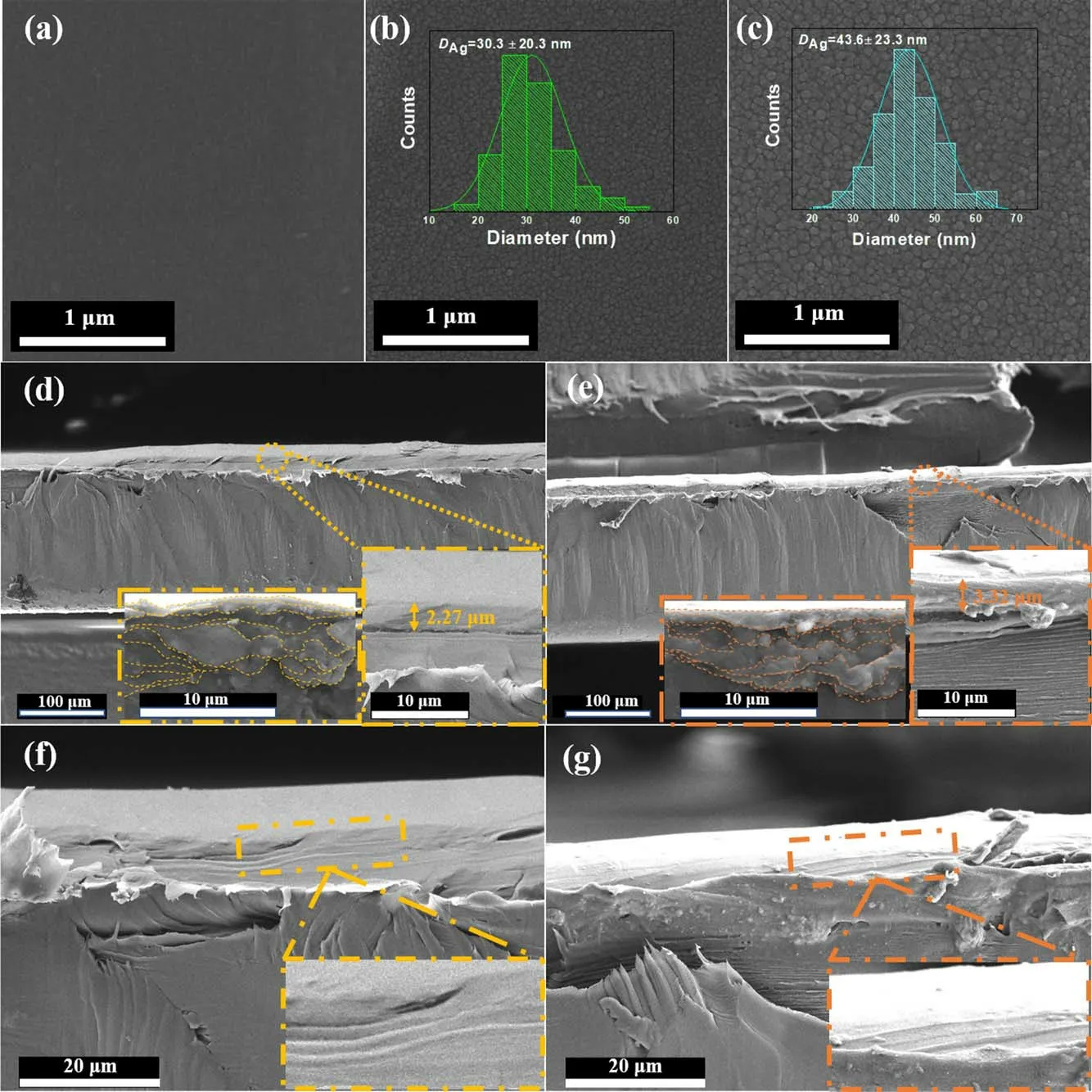
Figure 6.SEM images of the surface and cross-section of the pristine sample, Ag/PET-1, and Ag/PET-2: (a) pristine PET, (b) Ag/PET-1 surface (inset: size histograms of AgNPs), (c) Ag/PET-2 surface (inset: size histograms of AgNPs), (d) Ag/PET-1 cross-section, (e) Ag/PET-2 cross-section, (f) interlayer structure of Ag/PET-1 and (g) interlayer structure of Ag/PET-2.
The EMI SE is a measure of a material’s ability to attenuate electromagnetic wave intensity.Most of the previous studies on EMI shielding focused on the special frequency range of 8.2-12.4 GHz [4, 19, 29, 30], which is the operating range for satellite communication, national defense tracking, and television signal transmission [68].However,there has been little research on EMI shielding in lower-frequency bands, such as frequency modulation (30-300 MHz),maritime/aviation communication, and short-range communication(0.3-1.0 GHz)[17,18,31].Therefore,it is of interest to investigate EMI shielding in these regions(0.01-1.0 GHz).

Figure 7.(a)-(c) The EMI SE of Ag/PET-1 and Ag/PET-2 as functions of the frequency in the range of 0.01-0.3 GHz: (a) EMI SET,(b) EMI SER, and (c) EMI SEA.(d)-(f) EMI SE of Ag/PET-1 and Ag/PET-2 as functions of the frequency in the range of 0.3-1.0 GHz:(d) EMI SET, (e) EMI SER, and (f) EMI SEA.
The total SE was calculated using the following equation[4, 8, 17, 21, 24, 28, 30]:

where PIand PTare the electromagnetic wave incident power and projection power, respectively.The total SE consisted of three parts: absorption (SEA), reflection (SER), and multiple internal reflections(SEMR).If SETwas greater than 15 dB,the SEMRvalue could be ignored.Therefore, the equation can be expressed as follows:
Thus,the total EMI SE depends on the combined action of surface reflection and internal absorption.Using a microwave vector network analyzer, SERand SEAcan be calculated from the reflection coefficient (R) and absorption coefficient (A) by the following equations:

Figure 8.Changes in the EMI SE measured at(a)0.01 and 0.03 GHz and (b) 0.3 and 1.0 GHz.
The R and T coefficients are determined by the scattering parameter (S), as follows:

where PI, PR, PA, and PTare the incident, reflected, absorbed,and transmitted power of the electromagnetic wave, respectively.Furthermore, the EMI SE has the ability to block electromagnetic waves and can be used to evaluate the EMI effect of materials.Therefore, the EMI SE (%) was calculated using the following equation:

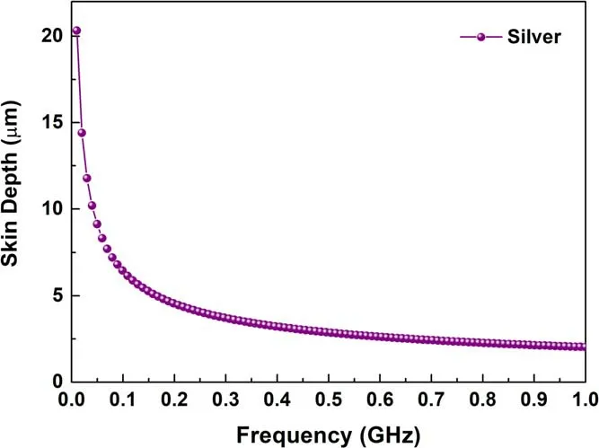
Figure 9.Skin depth of silver as a function of frequency in the range of 0.01-1.0 GHz.
Figures 7(a)-(c)and(d)-(f)show the total EMI(SET),EMI by absorption (SEA), and EMI by reflection (SER) of the Ag/PET-1 and Ag/PET-2 patterns in the ranges of 0.01-0.3 and 0.3-1.0 GHz, respectively.Generally, the EMI SE value is evaluated in decibels (dB).The higher the EMI SE value, the lower the incident wave energy that can be transmitted.As is well known,when the EMI SE value is 20 dB,it indicates that 99% of the electromagnetic radiation can be effectively shielded,which is the index of commercial EMI shielding materials.Meanwhile, when the EMI SE value is 30 dB, the corresponding SE is 99.9%, which makes it applicable in advanced application fields, such as medical treatment and military equipment[4,19,21,28,69].Comparing the two samples, the SETvalues of Ag/PET-2 reached 39.45, 38.16,34.39, and 31.56 dB at 0.01, 0.03, 0.3, and 1.0 GHz, respectively.However, for Ag/PET-1, the SETvalues were 36.35,35.12, 31.33, and 28.47 dB at 0.01, 0.03, 0.3, and 1.0 GHz(figure 8),respectively.Meanwhile,different attenuation trends were evident at 0.01-0.3 and 0.3-1.0 GHz [17, 18, 31], which can be regarded as a measure of the effective shielding[70,71].The more stable the variation,the more significant the effective EMI SE.Moreover, an increase in the silver film thickness led to a significant increase in SEAand SER, but benefited SERin the range of 0.3-1.0 GHz [16, 20, 21].Remarkable changes in the reflection and approximately the same absorption were observed,indicating that the cell-like morphology of the surface and layer-by-layer-like microstructure of the inside exhibited EMI shielding effects with reflection as the main component.Since the SERonly occur on the surface of thin silver film,the roughness of the silver film plays an important role in the SER.This indicated that the silver film in Ag/PET prepared by the surface DBD cold plasma is rough,which was also observed by Oh et al [43].Meanwhile, the remarkable changes of SEAare attributed to the conductivity of the silver film.In spite of these,a stable variation in SETwas observed,suggesting that the Ag/PET samples exhibited effective EMI SE property.Furthermore, from 0.01 to 0.3 GHz, especially at lower frequencies(0.01-0.05 GHz), absorption was found to play a major role in the EMI shielding, which was attributed to the increase in the shielding thickness[1,15,19,22,30,32].Therefore,we expect conductive filled composites with adaptive thicknesses(close to the skin depth theory of the material) [18, 31].
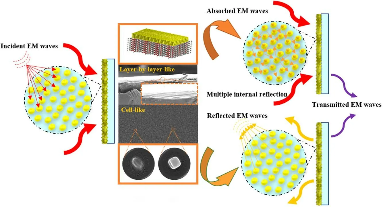
Figure 10.Schematic diagram of the EMI shielding mechanism of the Ag/PET sample.
Skin depth is the thinnest limit of electromagnetic wave shielding materials.It marks the entry thickness when the electromagnetic wave enters the material and its electric field intensity drops to 1/e of the incident intensity, which plays a significant role in the EMI shielding effectiveness.The skin depth of any material can be calculated by the following formula [71, 72]:

where ρ, μ, and f are the resistivity (Ω·m), permeability(Henries(H) = Ω·s, μ0= 4π × 10−7H m−1), and frequency (GHz).
Based on the theoretical data of silver, when the frequency was in the range of 0.30-1.0 GHz (microwave)(figure 9), the skin depth was 3.73-2.03 μm.When the frequencies were 0.01 and 0.03 GHz,the skin depths were 20.32 and 11.77 μm, respectively, which means that the lower the frequency, the higher the demand of the shielding thickness[8,18].It has to be noted that the performance was performed in the appearance of the silver film and PET.Therefore, the filling factor(maximum 50%)was not considered.Compared with Ag/PET-1 and Ag/PET-2,the obtained thickness of the silver film was consistent with the theoretical skin depth in the range of 0.3-1.0 GHz, showing a gentle attenuation trend,which was proven to form an effective shield [27, 73].
Schematic diagram of the EMI shielding mechanism of the Ag/PET sample is illustrated in figure 10.Both the electrically conductive networks of the surface cell-like configurations and the layer-by-layer-like structure of the crosssection endowed the Ag/PET with a high EMI SE[70,74].It has been reported that cell-like configurations contribute to increasing EMI SE via reflection and absorption in the cells[15, 19, 30, 74].Therefore, in the cell-like network on the surface of the silver film,the PVP fills the spaces between the AgNPs as the voids, which builds electrically conductive channels and enhances the dispersity of the AgNPs, forming compactly arranged microstructures as well [19, 22].In addition, when the incident electromagnetic wave impinges on the conducting plane, the obtained densely arranged AgNPs with preferentially oriented microstructures can be used as the surface reflection center, displaying a powerful reflection effect [46].Meanwhile, the carrier of the AgNPs forms an oscillation current and flows through the gap,which is beneficial for obtaining a better absorption effect [3, 32].From the perspective of the cross-section,based on the layerby-layer-like stacking structure of the silver films, multiple reflection and scattering effects will occur between layers,which is helpful for obtaining higher EMI shielding[30,31,46].Furthermore,the EMI SE value is proportional to the thickness of the shielding film, which can be reasonably adjusted and controlled according to the skin depth of the material [8, 18, 31].In summary, the obtained Ag/PET sample had an excellent surface morphology and internal structure, which exhibited superb microwave shielding performances under a low-loading condition of the filler.
4.Conclusion
A surface modification method of SAPGD with APSDBD reduction preparation method was applied to prepare Ag/PET for the first time.We adopted a simple, fast, and green synergistic strategy, with the aid of the efficient morphology control effect of the PVP capping agent,under the conditions of ultralow loading (0.022 wt%), to successfully synthesize the silver thin films.The obtained silver films existed in the form of pure silver, exhibiting a cell-like morphology with a closely arranged preferred orientation of the surface and forming a layer-by-layer-like superimposed microstructure inside, which benefited SER.Moreover, the obtained composite materials reached the theoretical material thickness(close to the skin depth of the material) with a high EMI SE(EMI SE > 30 dB in the range of 0.01-1.0 GHz).The mechanisms for optimizing the shielding performance revealed the significant fundamental basis for designing high reflection-dominated EMI shielding composites,providing an effective strategy for manufacturing metal or alloy films on surfaces of heat-sensitive materials (such as plastics and biological materials) at a relatively low cost.
Acknowledgments
This work is supported by National Natural Science Foundation of China (Nos.52077024, 21773020, 21673026,11505019),Natural Science Foundation of Liaoning Province(No.20180550085),and Zhang Xiuling Innovation Studio of Dalian City.
ORCID iDs
猜你喜欢
杂志排行
Plasma Science and Technology的其它文章
- Numerical simulation of laser-induced plasma in background gas considering multiple interaction processes
- Kinetic-theory-based investigation of electronegative plasma-wall transition with two populations of electrons
- Investigation of the fast magnetosonic wave excited by the Alfvén wave phase mixing by using the Hall-MHD model in inhomogeneous plasma
- The theoretical study on intermittency and propagation of geodesic acoustic mode in L-mode discharge near tokamak edge
- Experimental study of sheath potential coefficient in the J-TEXT tokamak
- Nonlinear evolution and secondary island formation of the double tearing mode in a hybrid simulation