RF magnetron sputtering induced the perpendicular magnetic anisotropy modification in Pt/Co based multilayers∗
2021-03-11RunzeLi李润泽YucaiLi李予才YuSheng盛宇andKaiyouWang王开友
Runze Li(李润泽), Yucai Li(李予才), Yu Sheng(盛宇), and Kaiyou Wang(王开友),3,4,†
1State Key Laboratory for Superlattices and Microstructures,Institute of Semiconductors,Chinese Academy of Sciences,Beijing 100083,China
2Center of Materials Science and Optoelectronics Engineering,University of Chinese Academy of Sciences,Beijing 100049,China
3Beijing Academy of Quantum Information Sciences,Beijing 100193,China
4Center for Excellence in Topological Quantum Computation,University of Chinese Academy of Sciences,Beijing 100049,China
Keywords: perpendicular magnetic anisotropy,RF magnetron sputtering,ion irradiation,spin orbit torque
1. Introduction
Current induced magnetization switching of perpendicular magnetic anisotropy (PMA) materials by spin orbit torque is promising for the next generation magnetoresistive random access memory (MRAM).[1–4]In the heavy metal/ferromagnetic metal(HM/FM)bilayer system,the PMA is sensitive to the HM/FM interface and FM can be switched by the spin current injected from the HM layer.[5–7]The critical switching current density and charge-to-spin conversion efficiency are dependent on the PMA in the HM/FM system.[8,9]PMA of thin films can be affected by various techniques:thermal annealing,ion irradiation,or oxidation.[10–17]In the previous works,these methods all need an additional process after the thin films growth to modify PMA.Therefore,it is essential to develop new effective ways to modify PMA of thin films.
Magnetron sputtering is a widely used method in thin films growth. Metals are generally deposited by direct current (DC) sputtering. However, for insulating target materials such as oxides and ceramics, there is a charge building up on the surface of the target with DC signal, which hinders the sputtering to proceed. By using a radio frequency(RF)source,the electrostatic charge can be discharged in each cycle, which allows the deposition of quality insulators such as AlOxand MgO. During RF magnetron sputtering, the deposited film is grounded and the target is connected to a RF power (13.56 MHz). The insulator target acts as a conductor for the RF alternating current field but also acts as an isolate for a self-induced DC field. When the target is anode,the deposited film will be irradiated by the positive ions in ignited plasma. Plasma during RF magnetron sputtering is mainly restrained near the target, thus the positive ion density on the target surface is higher than that on the deposited film surface.Even so,the magnetic properties of the deposited film can be affected by this ion irradiation. To our knowledge,few works have taken this effect into consideration.[18,19]
In this work, we investigate how the magnetic properties could be engineered by the RF magnetron sputtering. We firstly demonstrated that the influence of ion irradiation during RF magnetron sputtering should not be neglected and PMA of the deposited film could be tailored. AlOxis widely used in the spintronic research,[1,2]so we chose AlOxas the insulator target to investigate the RF magnetron sputtering effect. Then we studied the underlying physical mechanisms of the PMA changes by SRIM simulation. Finally, the influences of RF magnetron sputtering on SOT induced magnetization switching were investigated.
2. Method
To investigate the influences of RF magnetron sputtering on the deposited magnetic film, we firstly deposited Ta(1)/Pt(4)/Co(0.8)/Ru(2) (the numbers are layer thicknesses in nm)thin films on thermally oxidized silicon substrates using a DC magnetron sputtering system. The AlOxlayer was subsequently deposited on these films in different RF magnetron sputtering time tRF(1–10 min) with RF power PRF=100 W. The base pressure of the sputtering system was less than 5×10⁻⁸Torr. The DC sputtering conditions for all the metallic layers were: Ar gas pressure of 0.8 mTorr and DC power of 30 W with the deposition rates between 0.01 nm/s and 0.02 nm/s. The Ar gas pressure of 2 mTorr and RF power of 100 W were used to deposit AlOxlayer with the deposition rate of 0.2 nm/min. Thus we can use the RF magnetron sputtering time tRFto represent the deposited AlOxlayer thickness.The samples were then patterned into Hall bars with the width of 10µm and the length of 50µm by standard photo lithography and Ar+ion milling,as shown in Fig.1(a). The Hall bar structure allows us to probe the ferromagnetic state of the devices by measuring the anomalous Hall effect(AHE).A small current of 100µA was used to detect the ferromagnetic states while minimizing the heating effect.
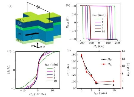
Fig.1. (a)Schematic of the studied magnetic multilayer system and the experimental measurements set-up for the Hall bar devices with the definition of x–y–z coordinates. (b) Out-of-plane magnetization hysteresis loops measured by AHE for devices deposited AlOx layer with tRF =0, 1, 2, 3, 10 min, respectively, at fixed PRF =100 W. (c) In-plane magnetization hysteresis loops measured by VSM. (d) Magnetic coercive field HC and anisotropy field HK obtained from(b)and(c)respectively as functions of tRF.
3. Result and discussion
Typical magnetic parameters (coercive and anisotropy fields)were deduced from the hysteresis loops to characterize PMA.Figure 1(b)shows the AHE hysteresis loops under the out-of-plane magnetic field. Clear square magnetic hysteresis loops were obtained for all the samples,indicating that all the films exhibit good perpendicular magnetic anisotropy even after RF magnetron sputtering. The same magnitude of the AHE resistance suggests the magnetization of all the samples can be fully reversed by the vertical magnetic field continuously. However,the coercive field HCof the devices decreases from 175 Oe to 95 Oe with increasing tRFfrom 0 to 3 min,which is shown in Fig.1(d). For devices with tRFfurther increasing up to 10 min, the HCis almost unchanged. Similar results in PMA Ta/Pt/Co/Pt and Ta/Pt/Co/Ti structures were also observed(details see supplementary Fig.S1). Anisotropy field HKis defined as the required minimum external magnetic field to fully align the magnetization along the hard axis.For Ta(1)/Pt(4)/Co(0.8)/Ru(2)structure,to obtain the relation between the magnetic anisotropy field HKand the variation of tRF, the magnetic hysteresis loops with the in-plane magnetic field swept between+15000 Oe and −15000 Oe for different samples were measured via a vibrating-sample magnetometer(VSM)at room temperature. The results are shown in Fig.1(c). Similar with HC,the determined HKdecreases dramatically initially and reduces to the half value of the sample without RF magnetron sputtering,which indicates the reduced PMA with increasing RF magnetron sputtering time. The HKthen keeps almost unchanged with tRFfurther increasing, as shown in Fig.1(d). The almost unchanged HKand HCfor the samples with tRF>3 min suggest that the impacts on the magnetic properties with further RF magnetron sputtering gradually diminish.
To identify the reason for this phenomenon, several experiments were performed. Firstly,we excluded the oxidation of Co atoms after deposition of the AlOx,x-ray photoelectron spectroscopy(XPS)spectra of the Co layer was measured for the deposited magnetic samples. No obvious difference is observed before and after the deposition of the AlOx(details see supplementary Fig.S2), which indicates that 2 nm thick Ru layer is sufficiently thick to prevent oxidation of the Co atoms.Secondly,we removed the upper AlOxlayer on the samples by the chemical etching technique and the hysteresis loops were subsequently measured again. The influences of the RF magnetron sputtering remained,thus the effect of interfacial stress was ruled out. Finally, the measured hysteresis loops for the structure of Ta/Pt/Co/Ru with different Ru thickness tRuwere shown in supplementary Fig.S3. The magnetic properties almost keep the same between the tRu=6 nm and tRu=2 nm samples,indicating that it is not the thickness of the top layer that modifies the PMA of the deposited film. Considering that these above factors were all excluded and ion irradiation induced PMA weakness has been observed in other works,[11,20]we believe that ion irradiation induced by RF magnetron sputtering is the main reason for the PMA modification in our experiments.
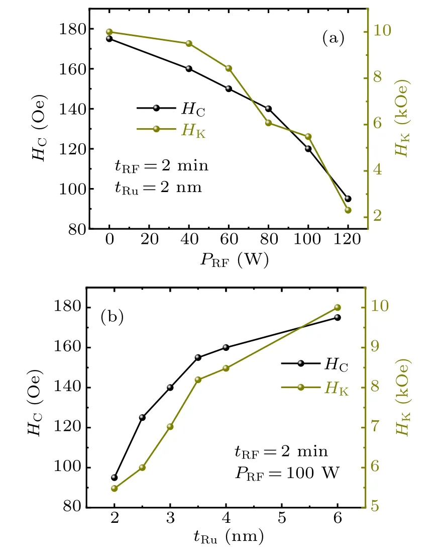
Fig.2. (a) The magnetic coercive field HC and anisotropy field HK against RF magnetron sputtering power PRF, with tRF = 2 min and tRu =2 nm. (b) HC and HK as functions of Ru layer thickness tRu,with tRF=2 min and PRF=100 W.
The irradiation energy of Ar+ions in plasma is related to the RF power. We expect a more significant reduction of the HCand HKwhen a higher RF magnetron sputtering power is used. Besides,a thicker Ru layer tRucan screen the irradiation effect more effectively. To verify our predictions, the AlOxlayer was deposited on Ta(1)/Pt(4)/Co(0.8)/Ru(2) magnetic thin films with different power intensities PRF(40–120 W)for 2 min. The DC self-bias potential is 160 V when PRF=40 W and linearly increases to 300 V when PRF=120 W. As presented in Fig.2(a), compared with the sample without AlOxcapping layer, the HCis reduced by 15 Oe and 80 Oe with PRF= 40 W and 120 W, respectively. In Fig.2, the HKwas measured by AHE and the detailed calculation process was shown in supplementary Fig.S4. Figure 2(a) shows that the HKalso decreases with the increasing PRF. When PRF=120 W,the HKreduces to 25%of the initial HKvalue.Then, the AlOxwas deposited with the fixed PRF=100 W and tRF=2 min on Ta(1)/Pt(4)/Co(0.8)/Ru(tRu)thin films with varying Ru layer thickness from 2 nm to 6 nm. As shown in Fig.2(b), with the increase of tRu, the reduction of HCand HKinduced by RF magnetron sputtering decreases,indicating that the Ar+ions irradiation effect is gradually screened by the thicker Ru layer.
To understand the underlying physical mechanisms of the PMA changes in our experiments, the ion irradiation in the RF magnetron sputtering process was modeled by Monte Carlo simulation programs(SRIM).[21,22]We used the grown Ta(1)/Pt(5)/Co(0.8)/Ru(2)structure for simulation. The damages in the deposited film caused by ion irradiation have two major terms: (I) displacement atoms, the atoms which are knocked off from their original normal lattice positions by an energetic Ar+ion; (II) vacancies, empty lattice sites caused by atoms’displacement.The DC self-bias potential was 300 V when PRF=120 W,thus ion irradiation energy EAr+=300 eV was set in the SRIM simulation. Although the fluence of Ar+ion irradiation on the target is much higher than that on the deposited film, we can estimate the ion fluence at the deposited film FSby the ion fluence at the target FTaccording to their relation. The RF source is a sinusoidal alternating current signal. If we ignore the influence of the transverse electromagnetic wave, FTcan be approximately calculated by the equation FT≈4PRFtRF/πVRFeA, where VRFis the DC selfbias potential, e is the charge of electron, and A is the area of the target. The shape of the plasma acting on the target surface is approximately a sphere, thus FScan be estimated by the equation FS≈(RT/RS)2×FT, where the distance between the plasma and the deposited film RSis 45 cm and the radius of the plasma sphere RTis 5 cm. The deposited AlOxlayer will make the ion irradiation have less influence on the Pt/Co/Ru structure. This can be equivalent to the shorter of the ion irradiation time, so we used a shorter simulation irradiation time compared to the time in the actual experiments.With the Ar+ion irradiation energy EAr+=300 eV and ion fluence FS=5.9×10¹⁶ions/cm2, the simulation results are shown in Fig.3. Figure 3(a)shows the distribution of the displacement Ru and Co atoms and figure 3(b)shows the spatial distribution of the vacancies in the Co layer. There are two mechanisms accounting for the PMA modification in our experiments. Firstly,some Ru atoms are driven into the Co layer by the irradiation process and the penetrated Ru atoms can subsequently bombard the Co atoms. As shown in Fig.3(a),although most Co atoms keep stay in the Co layer,part of the Co atoms can be bombarded into the Pt layer. The PMA of Pt/Co/Ru is strongly dependent on the Pt/Co interface quality,thus atoms intermixing at the Pt/Co interface can result in a weaker PMA.[23]Secondly, the magnetic properties of Pt/Co films depend on not only the Pt/Co interface,but also the structure of the Co layer as well. Defects such as interstitial atoms and vacancies in the Co layer will change the magnetic domain structure of the Co layer.[24–26]At the places irradiated,the magnetic domains would be more easily switched by the external magnetic field,which has been confirmed in previous study of the Pt/Co/Pt films.[11]Therefore,the weakened PMA of Pt/Co/Ru multilayers can be explained by the atoms intermixing at the Pt/Co interface and the change of the magnetic domain structure in the Co layer. Considering that the PMA of the Pt/Co based thin films can be affected by RF magnetron sputtering, the SOT induced magnetization switching should be influenced as well.
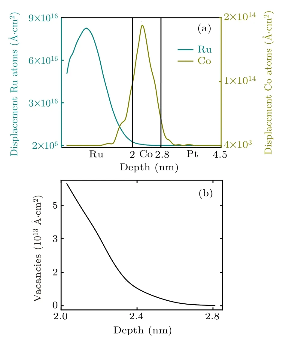
Fig.3. The simulated results of SRIM. (a) Displacement Ru and Co atoms distribution after Ar+ ion irradiation with ion irradiation energy EAr+ =300 eV and ion fluence F =5.9×10¹⁶ ions/cm2. (b)Vacancy number distribution in Co layer after Ar+ ion irradiation.
As shown in Fig.4(a), current pulse induced magnetization switching for devices Ta(1)/Pt(4)/Co(0.8)/Ru(2)/AlOx(tRF)was investigated. Every 2 seconds, a pulse current Ipulsewith duration of 15 ms was injected to the devices. RHallwas measured by a low current of 100µA after each pulse to probe the magnetization state. Because of the spin Hall effect(SHE)in the Pt layer,the charge current in the x direction gives rise to a spin current in the out-of-plane direction, with the spin orientation along the y direction. The spin current is absorbed by the adjacent Co layer,resulting in both a damping-like torque τ‖~m×y×m and a field-like torque τ⊥~m×y,where m is the unit vector that denotes the magnetization direction. Neither torque possesses an up-or down-direction preference.But if an external magnetic field is applied collinearly to the current,the symmetry in the response to the SHE torque is broken and the magnetization can be deterministically switched.[4]For our devices,an external magnetic field HX=−300 Oe is applied along the −x direction, thus positive currents favor a positive magnetization(resulting in a positive Hall resistance),while negative currents favor a negative magnetization.
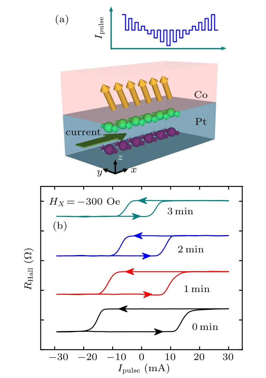
Fig.4. (a) Illustration of the spin Hall effect in the Pt layer with an external magnetic field of HX =−300 Oe. (b) Current pulse induced magnetization switching for the devices with tRF=0,1,2,3 min.
The current induced magnetization switching loops for the devices with tRF=0, 1, 2, 3 min are shown in Fig.4(b).The threshold current intensity Ithdecreases with increasing tRF, which is consistent with the fact that PMA of the thin films is weakened after RF magnetron sputtering. However,the magnitude of the maximum anomalous Hall resistance becomes smaller with tRF≥2 min, which is different from the constant maximum anomalous Hall resistance reversed by the vertical magnetic field. In our experiments, the samples exhibit a multi-domain structure,thus the magnetization reversal process is dominated by magnetic domain propagation.[27,28]Considering there is spatial inhomogeneity, the domain walls would be easily nucleated in the more seriously irradiated area.On the other hand, after RF magnetron sputtering, defects in the Co layer and degradation of the Pt/Co and Co/Ru interfaces can act as pinning centers. When tRF=1 min, the influence of these pinning centers was not strong. The critical switching current density decreased and a full SOT induced magnetization switching could be achieved. For more serious irradiated devices with tRF=2, 3 min, SOT cannot induce a full magnetization switching. The reason might be that the pinning centers hinder parts of the magnetic domains to be switched by SOT,which results in the smaller Hall resistance. We have also investigated the difference in magnetic domains switching process after RF magnetron sputtering by polar magnetooptical Kerr effect(MOKE)measurement technique. The experiment results are shown in Fig.S5 in supplementary materials,which suggests that the magnetic domains in the irradiated area become more easily to be nucleated and reversed,which is in good agreement with the current induced magnetization switching.
4. Conclusions
In summary, AlOxwas deposited on Pt/Co/NM type structures by RF magnetron sputtering technique. We found that ion irradiation during RF magnetron sputtering can weaken the PMA of the deposited films. Using a smaller RF magnetron sputtering power and increasing the thickness of the NM layer can reduce the impacts of this ion irradiation.The simulation results of SRIM indicate that the degradation of the Pt/Co interfaces and the increasing defects in the Co layer can account for the PMA weakness. In the SOT induced magnetization switching process, both the Hall resistance and the threshold switching current density decreased after RF magnetron sputtering. Our results will attract the attention of the RF magnetron sputtering and may lead to innovative spintronic applications.
猜你喜欢
杂志排行

Chinese Physics B的其它文章
- Novel traveling wave solutions and stability analysis of perturbed Kaup–Newell Schr¨odinger dynamical model and its applications∗
- A local refinement purely meshless scheme for time fractional nonlinear Schr¨odinger equation in irregular geometry region∗
- Coherent-driving-assisted quantum speedup in Markovian channels∗
- Quantifying entanglement in terms of an operational way∗
- Tunable ponderomotive squeezing in an optomechanical system with two coupled resonators∗
- State transfer on two-fold Cayley trees via quantum walks∗