Performance analysis of GaN-based high-electron-mobility transistors with postpassivation plasma treatment∗
2021-03-11XingYeZhou周幸叶XinTan谭鑫YuanJieLv吕元杰GuoDongGu顾国栋ZhiRongZhang张志荣YanMinGuo郭艳敏ZhiHongFeng冯志红andShuJunCai蔡树军
Xing-Ye Zhou(周幸叶), Xin Tan(谭鑫), Yuan-Jie Lv(吕元杰), Guo-Dong Gu(顾国栋),Zhi-Rong Zhang(张志荣), Yan-Min Guo(郭艳敏), Zhi-Hong Feng(冯志红), and Shu-Jun Cai(蔡树军)
National Key Laboratory of Application Specific Integrated Circuit,Hebei Semiconductor Research Institute,Shijiazhuang 050051,China
Keywords: GaN,HEMT,gate leakage,trapping effect
1. Introduction
Owing to the advantages of material properties, such as high electron mobility,high breakdown electric field,and high thermal conductivity,GaN-based high-electron-mobility transistors (HEMTs) have attracted lots of interest and achieved excellent successes in the past few years.[1–4]However, further performance improvements of these devices are limited by high gate leakage and small gate swing.[5,6]The gate leakage in AlGaN/GaN HEMTs and InAlN/GaN HEMTs have been widely investigated.[7–16]For device fabrication, surface passivation is usually adopted,which can effectively suppress the I–V hysteresis and current collapse induced by trapping effect in the access region. Nevertheless,the gate leakage will probably increase after passivation,[17,18]which is unexpected.
In this paper, AlGaN/GaN HEMTs with postpassivation plasma treatment are investigated for the first time. Comparing with the conventional devices, the results demonstrate that the gate leakage is greatly reduced, while the drain current is increased for AlGaN/GaN HEMTs with postpassivation plasma treatment. In order to study the influence of postpassivation plasma treatment on the surface and interface traps,capacitance–voltage measurement and frequency-dependent conductance method are used. It is shown that the improvement of direct current(DC)characteristics of devices is due to minimizing the virtual gate effect, which can be attributed to the suppression of surface traps in the access region by postpassivation plasma treatment. Moreover,the density and time constant of interface traps under the gate are also extracted and analyzed.
2. Device structure and fabrication

Fig.1. Schematic cross-sectional structure of AlGaN/GaN HEMT.
The AlGaN/GaN epi-layer structure in this work was grown by metal–organic chemical vapor deposition(MOCVD) on SiC substrate, which was composed of a 2-µm-thick undoped GaN layer, a 1-nm-thick AlN inserting layer and a 26-nm-thick Al0.2Ga0.8N barrier layer.A two-dimensional electron gas (2DEG) with a density of 8.84 ×1012cm−2and an electron mobility of 2066 cm2·V−1·s−1was obtained based on the roomtemperature Hall measurement. For the device fabrication,the mesa isolation was formed first by inductively coupled plasma (ICP) dry etching. Source/drain electrode contacts with Ti/Al/Ni/Au metal stack formed,followed by rapid thermal annealing at 810◦C for 30 s in N2atmosphere. After that,the gate electrode with Ni/Au(50/200 nm)stack was deposited by electron-beam evaporation. For passivation, 100-nm-thick SiNxlayer was grown by plasma enhanced chemical vapor deposition (PECVD) with SiH4/NH3(200/3 sccm) under an RF power of 20 W at 250◦C. Then, the SiNxlayer in the electrode contact region was opened by ICP etching.After removing the photoresist, the O2plasma treatment on the wafer was finally carried out with an RF power of 50 W for 3 min in a plasma treatment system. In order to investigate the traps by using capacitance–voltage measurement and frequency-dependent conductance method,an FAT device was fabricated in this work. The gate length and width were Lg=20µm and W =100µm,respectively. The gate–source spacing was 10 µm with a drain–source distance of 100 µm.The schematic cross section structure of AlGaN/GaN HEMT is shown in Fig.1.
3. Results and discussion
First, the direct current(DC)characteristics of the fabricated AlGaN/GaN HEMT are measured as plotted in Fig.2.Figures 2(a)–2(c)show the comparison of gate leakage,transfer and output characteristics between devices with and without postpassivation plasma treatment, respectively. As seen from Fig.2, the gate leakage is reduced by almost 3 orders of magnitude compared with that of the device without postpassivation plasma treatment. In addition, the drain current increases after the devices have been plasma-treated. The performance improvement may be due to the suppression of trapinduced virtual gate effect, which will be discussed in detail below.

Fig.2. Comparison of DC characteristics between AlGaN/GaN HEMT with and without plasma treatment,showing(a)gate leakage,(b)transfer characteristics,and(c)output characteristics.
Capacitance–voltage measurements with different frequencies are carried out,the results are shown in Fig.3,where the C–V curves are obtained by using gate and source contact. It can be seen from Fig.3(a)that there exists frequencydependent capacitance dispersion in HEMT without plasma treatment, indicating a trapping effect. With the postpassivation plasma treatment,the capacitance dispersion is negligible[see Fig.3(b)]. As is well known,the traps at the 2DEG interface can cause the threshold voltage to shift. However, there is observed no threshold voltage Vthdispersion in devices with or without plasma treatment. This means that the capacitance dispersion at zero or low reverse voltage for devices without plasma treatment may be induced by the traps in the access region. The postpassivation plasma treatment can reduce the surface traps in the access region, consequently leading the capacitance dispersion to be suppressed. Moreover, the decrease of gate leakage current in Fig.2 can also be attributed to the reduction of surface traps,where the surface leakage path is blocked due to the postpassivatioin plasma treatment. The postpassivation plasma treatment in this work may change the composition of SiNxpassivation layer. For example,the dangling bonds may be reduced or the nitrogen vacancies may be filled with oxygen atoms, thereby reducing the surface traps and blocking the leakage path in the access region.
Based on the C–V measurement results in Fig.3, the 2DEG density under the gate of AlGaN/GaN HEMT can be calculated by following the algorithm in Ref. [19]. Figure 4 shows the calculated values of 2DEG density in AlGaN/GaN HEMT with and without the postpassivation plasma treatment.We can see that the 2DEG density increases after postpassivation plasma treatment. This can be explained by the trapsinduced virtual gate effect.For the AlGaN/GaN HEMTs without the postpassivation plasma treatment, there are more surface traps in the access region, which can act as a virtual gate. The virtual gate will result in the reduction of 2DEG density, since the 2DEG density is dependent on the Schottky gate area.[19,20]With the postpassivation plasma treatment,the surface traps are effectively suppressed and thus the virtual gate effect is minimized. Consequently,the 2DEG density increases,which is consistent with the increase of drain current(see Fig.2).
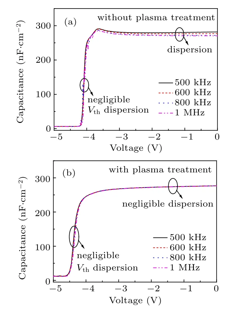
Fig.3. Capacitance–voltage measurement results of AlGaN/GaN HEMT(a)without and(b)with postpassivatioin plasma treatment.

Fig.4. Density of 2DEG versus voltage, obtained from C–V measurement for AlGaN/GaN HEMT with and without plasma treatment.Finally, the interface trap density under the gate is extracted by the frequency-dependent conductance method. The small-signal equivalent circuits for frequency-dependent conductance measurement are shown in Fig.5. The resistance Rit and capacitance Cit in Fig.5(a) represent the interface traps with a time constant τit=Rit·Cit. Figure 5(b)shows the simplified circuit with a parallel capacitance Cp and conductance Gp. Under the assumption of continuous trap levels,the conductance Gp can be expressed as[21,22]
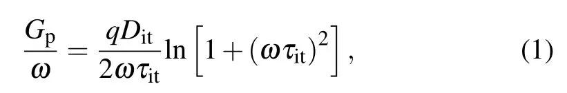
where ω =2π f is the radial frequency,Ditis the trap density,and τitis the trap time constant.
Figure 6(a)shows the measurement results of frequencydependent conductance Gpas a function of ω under different gate bias voltages for the AlGaN/GaN HEMT with the postpassivation plasma treatment, where the fitting results from Eq. (1) are also plotted. It can be seen that the model fitting results match the experimental data very well. The extracted interface trap density mapping is given in Fig.6(b),and the interface traps exhibit short time constant.Therefore,the threshold voltage will not be affected by the fast interface traps,leading to the negligible frequency-dependent Vthshift in Fig.3.
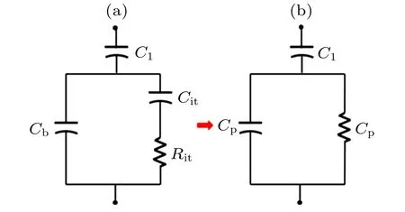
Fig.5. Small-signal equivalent circuits for frequency-dependent conductance measurement,showing(a)gate capacitor with interface traps,and(b)simplified circuit used in conductance-based Dit analysis.

Fig.6. Frequency-dependent conductance measurements of AlGaN/GaN HEMTs with postpassivation plasma treatment: (a) conductance as a function of radial frequency and (b) extracted trap density as a function of time constant.
4. Conclusions
In this work, AlGaN/GaN HEMTs with postpassivation plasma treatment are fabricated and investigated. It is demonstrated that comparing with the conventional devices,the gate leakage is effectively reduced, while the drain current is increased for AlGaN/GaN HEMTs with postpassivation plasma treatment. The surface and interface traps are studied based on the capacitance–voltage measurement and frequency-dependent conductance method. The improvement of DC characteristics of devices can be attributed to the suppression of virtual gate effect by the postpassivation plasma treatment. The results in this work can provide a reference for improving the performances of AlGaN/GaN HEMTs.
杂志排行

Chinese Physics B的其它文章
- Novel traveling wave solutions and stability analysis of perturbed Kaup–Newell Schr¨odinger dynamical model and its applications∗
- A local refinement purely meshless scheme for time fractional nonlinear Schr¨odinger equation in irregular geometry region∗
- Coherent-driving-assisted quantum speedup in Markovian channels∗
- Quantifying entanglement in terms of an operational way∗
- Tunable ponderomotive squeezing in an optomechanical system with two coupled resonators∗
- State transfer on two-fold Cayley trees via quantum walks∗