Modulation of the second-harmonic generation in MoS2 by graphene covering∗
2021-03-11ChunchunWu吴春春NianzeShang尚念泽ZixunZhao赵子荀ZhihongZhang张智宏JingLiang梁晶ChangLiu刘畅YonggangZuo左勇刚MingchaoDing丁铭超JinhuanWang王金焕HaoHong洪浩JieXiong熊杰andKaihuiLiu刘开辉
Chunchun Wu(吴春春), Nianze Shang(尚念泽), Zixun Zhao(赵子荀), Zhihong Zhang(张智宏),Jing Liang(梁晶), Chang Liu(刘畅), Yonggang Zuo(左勇刚), Mingchao Ding(丁铭超),Jinhuan Wang(王金焕), Hao Hong(洪浩),‡, Jie Xiong(熊杰), and Kaihui Liu(刘开辉),¶
1State Key Laboratory of Electronic Thin Films and Integrated Devices,University of Electronic Science and Technology of China,Chengdu 610054,China 2State Key Laboratory for Mesoscopic Physics and Frontiers Science Center for Nano-optoelectronics,Collaborative Innovation Center of Quantum Matter,Academy of Advanced Interdisciplinary Studies,School of Physics,Peking University,Beijing 100871,China
3Institute of Physics,Chinese Academy of Sciences,Beijing 100080,China
Keywords: two-dimensional materials,second harmonic generation(SHG),graphene,dielectric screening
1. Introduction
Group VI transition-metal dichalcogenides (TMDs), the representative two-dimensional (2D) materials, have brought us plentiful physics,including strongly bound excitons,valleyselective circular dichroism, 2D topological insulating states,etc.[1–11]Among these exciting physical properties, efficient nonlinear optical responses, ranging from second harmonic generation (SHG) to high harmonic generation (HHG) have been found in these atomically thin layered materials and attracted tremendous scientific interests.[12–17]These strong nonlinear optical responses are the fundamental building blocks in the design of advanced optics devices and also bring us unique techniques in material characterization.[18–21]Manipulation and engineering of the nonlinear properties of 2D materials are of paramount importance for realizing practical devices. Previously, some methods have been proposed to achieve the modulation of nonlinear optical response in 2D materials,including coupling with waveguides,suffering electron doping or in-plane strain,etc.[22–30]However,those methods are either complicated in fabrication processes or limited by specific substrates. Therefore, new mechanisms for facile and efficient nonlinear optical response manipulation are still on the way for further exploration.
Van der Waals interfacial engineering is supposed to be an efficient approach to modulate the physical properties of 2D materials. Benefiting from the atomically thin structure,the electron wave functions of 2D materials are distributed at the surface, leading to their sensitive responses to interfacial interaction such as the van der Waals forces.[31]Recent works have revealed their tunability in electronic,mechanical,optical properties by van der Waals stacking.[32,33]For examples,flat band and superconductivity were observed in bilayer graphene with specific twist angle,[34]and moir´e excitons emerged in TMDs heterostructures.[35–38]More intriguing phenomenon has also been discovered in twisted bilayer heterojunction,including bandgap opening in graphene with adhering hexagonal boron nitride (h-BN),[39–41]and strong electron–phonon interaction at TMDs/h-BN interface.[42]Previously, the SHG from TMDs bilayer/heterostructures has been explored,which can be descried by the vector superposition of the SHG electric fields from the individual components.[43]However, direct modulation of nonlinear optical properties of one layer by another with van der Waals interaction remains largely unexplored.
In this article, we demonstrate that the nonlinear optical responses of 2D materials can be efficiently modulated by exciton oscillator strength under resonant excitation through the modification of the local dielectric environment. Moreover,with restraining the excitons formation by electron doping,this SHG modulation behavior will become faint, exhibiting appealing flexibility in the real device application designing.
2. Methods
Synthesis of MoS2MoS2monolayer samples were grown on SiO2substrate with 300 nm. 10 mg of MoO3(99%,Sigma-Aldrich)powder and 2 mg of NaCl(Greagent,99.95%)were mixed and placed at the center of a tube furnace and 1 g of sulfur (99%, Sigma-Aldrich) powder was placed upstream of a quartz tube. The SiO2substrate was placed downstream 8 cm away from the Mo source. The chamber of the furnace was then flushed with argon for an inert atmosphere and subsequently ramped up to the optimized growth temperature(~780◦C)with 100 sccm argon. During growth process,the temperature for sulfur evaporation was ~115◦C.The entire process was carried out under ~150 Pa and the growth duration was set as 10 min. After the growth,the system was naturally cooled to room temperature.
Heterostructure preparationMoS2was grown on SiO2substrate by chemical vapor deposition method. The graphene monolayer,graphene few-layer,and h-BN were mechanically exfoliated directly on PDMS films. Then, we stamped the PDMS films on the Si/SiO2substrate with MoS2and slowly released the PDMS.Contacts to the monolayer graphene flake were made using electron-beam evaporation.
PL and Raman measurementsAll the PL and Raman data were measured by self-built experimental equipment with 532 nm CW solid-state laser. The integral time was set as 5 s for PL measurements and laser power was set as 1 mW. The integral time was 60 s for the Raman measurements under the excitation of 2 mW laser power.
SHG measurementsWavelength-dependent SHG spectra were measured by using Coherent Vitara-T oscillator and optical parametric amplifier(OPA)9850 laser system(~70 fs,250 kHz,1200–1600 nm)excitation. Excitation laser was focused by a Nikon objective (60×, NA=0.65) and the SHG signal was collected by the same Nikon objective with reflection mode.Through filtering out the excitation laser with a 700 nm short pass filter, SHG signal was recorded by the Princeton SP2500 spectrometer equipped with a nitrogen cooled Si charge coupled devices(CCD).All the experiments were done at room temperature.
3. Results and discussion
In this work, mechanical exfoliated graphene monolayer was transferred onto chemical vapor deposition(CVD)grown MoS2monolayer on 300 nm SiO2/Si substrate via dry transfer method(Fig.1(b)). The samples were firstly characterized via Raman and photoluminescence(PL)spectra(Fig.S1). In the Raman spectrum of individual MoS2and graphene, the standard characteristic peak position and intensity indicate their high quality and monolayer nature. The Raman intensity of MoS2is enhanced by ~1.5 times in the heterostructure,indicating a clean and strongly coupled interface.[44]This interfacial coupling effect can also be observed in the PL spectra,where the PL intensity in MoS2/graphene heterostructure is quenched to 10%because of electronic coupling and the associated charge/energy transfer process.[44]
The nonlinear optical response of monolayer MoS2was investigated in the atmosphere at room temperature. Under excitation with fundamental frequency ω, the strong secondorder susceptibility χ2ωof MoS2leads to nonlinear polarization P2ω=ε0χ2ωEωEωand distinct SHG response. As expected, under femtosecond excitation at 1300 nm, a reflected SHG signal with peak centered at 650 nm was collected(Fig.1(c)). This frequency harmonic generation phenomenon arises from the up-conversion process which requires instantaneous capture of two near-infrared photons to generate a visible photon. Therefore, the radiated SHG intensity obeys a squared dependence on the fundamental excitation power as shown in Fig.1(d), where a double-logarithm representation is used for clarity.
Figures 2(a) and 2(b) show the SHG spectra of MoS2and MoS2/graphene heterostructure, where totally different behaviors are exhibited under different wavelength excitation. For 1326 nm excitation, the SHG peak intensity of MoS2/graphene weakened to 45%compared with that of pristine MoS2(Fig.2(a)). However, the SHG peak intensity enhanced to 130% in the MoS2/graphene heterostructure with excitation wavelengths of 1420 nm (Fig.2(b)). As graphene monolayer is inversion symmetric, the second-order optical nonlinearity is electric-dipole forbidden and no SHG signal can be generated. Therefore,the variation of SHG must stem from the modulation of MoS2by graphene covering.
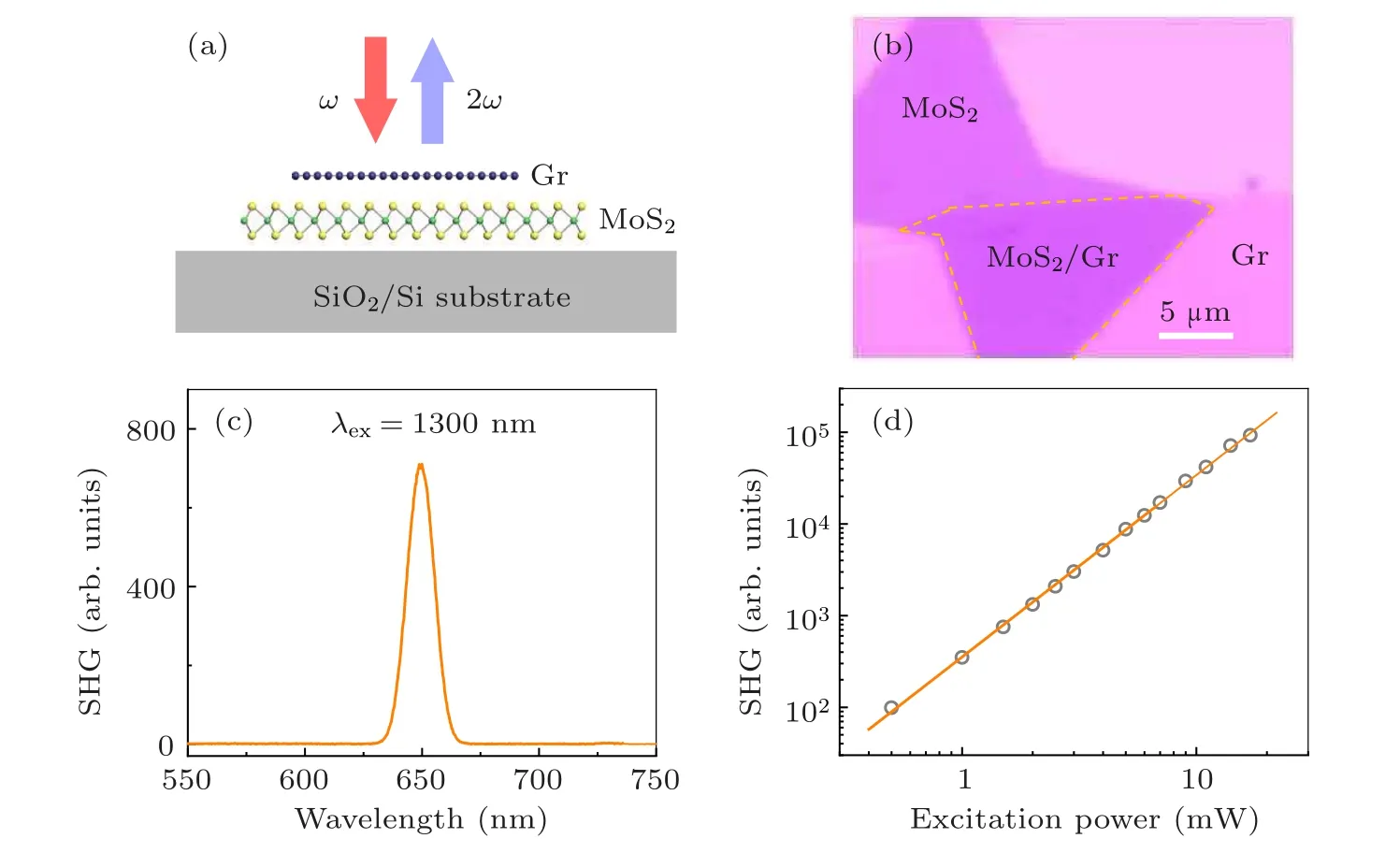
Fig.1. SHG in MoS2/graphene heterostructure. (a) Schematic illustration of optical SHG experiments on MoS2 monolayer and MoS2/graphene heterostructure. (b) Optical image of MoS2/graphene. Exfoliated monolayer graphene was transferred on the top of CVD grown monolayer MoS2 forming MoS2/graphene heterostructure(in dashed line). Scale bar is 5µm. (c)Optical SHG spectrum of MoS2 monolayer under excitation of 1300 nm.(d)The power dependence of SHG peak intensity shows the expected quadratic dependence.
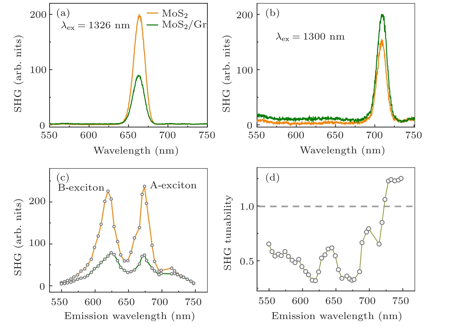
Fig.2.Wavelengthdependent SHG modulation in MoS2/graphene heterostructure.(a)Optical SHG spectra of monolayer MoS2 and MoS2/graphene heterostructure under excitation of 1326 nm, where the SHG decreased to 45% in the heterostructure. (b) SHG spectra of MoS2 monolayer and MoS2/graphene heterostructure under excitation of 1420 nm,where the SHG enhanced up to 130%in the heterostructure.(c)Wavelength-dependent SHG intensity of monolayer MoS2 and MoS2/graphene heterostructure. Both curves show peaks around MoS2 A-exciton and MoS2 B-exciton.(d) The SHG tenability, which describes the SHG intensity of MoS2/graphene to that of MoS2, is plotted. With interfacing graphene, the SHG intensity attenuated to ~30%under resonance excitation,while slightly enhanced under off-resonance excitation.
To further understand this SHG engineering performance,we measured the excitation wavelength dependent SHG spectra of MoS2/graphene heterostructure and MoS2monolayer with tuning excitation wavelengths (Fig.2(c)). All the two wavelength dependent curves feature two prominent peaks at 675 nm and 620 nm, corresponding to A-exciton and Bexciton of MoS2, respectively.[1]Under resonance excitation of exciton states, the SHG intensity is significantly enhanced due to the enhanced light–matter interaction and exciton dipole with strong oscillator strength.[13]The SHG tunability, which is defined as the ratio of the SHG intensity in MoS2/graphene to that in pristine MoS2,is plotted in Fig.2(d).Wavelength dependent SHG tunability shows that the onresonance excitation of exciton brings SHG intensity abatement while off-resonance excitation gives SHG intensity enhancement after graphene covering.
This on-resonance SHG weakening can also be gate tunable. Figure 3(a) shows the schematic diagram of our device, where ion-gel gating was used to controllably tune the chemical potential of the sample. By applying positive gate voltage Vg, the heterostructure will be electron doped, while negative gate voltage means hole doped. As our CVD grown MoS2samples are electron doped in nature, the application of a negative gate voltage will bring MoS2to charge neutral(Fig.S2). As expected,SHG spectra of both monolayer MoS2and MoS2/graphene heterostructure show significant gate tunability under on-resonance excitation of 1340 nm (Fig.S3).Their SHG intensity reaches the maximum at Vg=−1 V,and show continuous decrease with voltage increase (Fig.3(b)).Figure 3(c)shows the gate-dependent SHG tunability of MoS2with graphene covering. The SHG tunability is about 43%when Vgis between −2 V and 0 V, where MoS2is chargeneutral and A-exciton dominates the optical properties. When Vggoes positive and the formation of charge-neutral exciton is suppressed,on-resonance SHG weakening becomes faint.
We first discuss the on-resonance SHG weakening after covering graphene monolayer. There are mainly three scenarios that could be responsible for this SHG weakening: energy/charge transfer, charge doping, and dielectric screening effect. Though charge/energy transfer process is a common cause for PL quenching, it seems not possible for nonlinear optical signal decrease observed here. The parametric SHG process, which occurs instantaneously during the excitation pulse (~100 fs in our experiments), is ahead the charge/energy transfer process which takes scores of picoseconds after photoexcitation.[44–46]Meanwhile, the charge/energy transfer process is generally excitation wavelength independent,which happens at both the band edge and deep band in MoS2. This is in contrast with the wavelengthdependent SHG modulation we observed. Charge doping can also be excluded from the primary causes, as the SHG intensity of MoS2without gating(Vg=0 V)is higher than that of MoS2/graphene at any doping level(Fig.3(b)).
Dielectric screening effect is believed to be the most reasonable mechanism that responds to the SHG weakening.With graphene covering,the interaction strength between electron and hole in an exciton decreases,resulting in a reduction in spatial overlapping in MoS2. As a result, the exciton oscillator strength would be diminished according to the Fermi golden rule(Fig.4(a)). Since the exciton effects mainly contribute to the SHG response under resonant excitation,the decrease of exciton oscillator strength with graphene covering will surely bring the wavelength-dependent SHG modulation where the SHG weakens under resonance excitation.
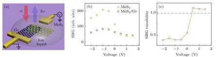
Fig.3. Gate-dependent SHG in MoS2 monolayer and MoS2/graphene heterostructure. (a)Schematic of gated MoS2/graphene via ion-gel. (b)Gate voltage dependent SHG in monolayer MoS2 and MoS2/graphene. As our CVD grown MoS2 is electron doped in nature,the application of negative gate voltage will bring MoS2 to charge neutral and decline SHG intensity for both MoS2 monolayer and MoS2/graphene heterostructure. (c)SHG tunability at different gate voltage. At negative gate voltage where MoS2 is charge-neutral, the SHG tunability can reach 43%. When the gate voltage goes positive and the formation of charge-neutral exciton is suppressed,SHG modulation behavior will become faint. SHG of monolayer MoS2 is nearly the same as that of heterostructure.
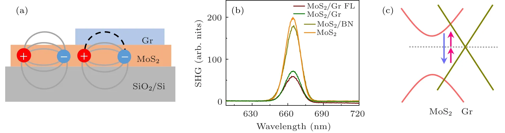
Fig.4. Mechanisms of SHG modulation in MoS2 by graphene covering. (a)Schematic illustration of dielectric screening effect in MoS2/graphene heterostructure. With graphene covering,the interaction strength between electron and hole in an exciton decreases,resulting in oscillator strength diminishing. (b)Optical SHG spectra of MoS2,MoS2/BN,MoS2/graphene,and MoS2/Gr few-layer under excitation of 1330 nm. Serving as strong screening dielectric material,graphene declines the SHG intensity of MoS2 monolayer to 35%at excitation resonance. For MoS2/Gr few-layer,the SHG further reduces to 30%. While for the covering of insulating h-BN,MoS2 SHG intensity only decreases to 90%. (c)Schematic of interlayer excitation SHG between MoS2 and graphene,which may response for the SHG enhancement under off-resonance excitation.
In the following, we used different dielectric materials to test the screening strength and modulate the SHG intensity. As graphene is semimetal with abundant free carriers and hence provides a strong dielectric screening, the SHG of MoS2monolayer weakens to ~35%after adhering monolayer graphene. While for the covering of insulating BN, MoS2SHG intensity only decreases to 90% (Fig.4(b)). Graphene few layers with stronger screening effect bring deeper SHG tunability to ~30%.
Afterwards, we elucidate the mechanism of SHG enhancement with graphene covering under off-resonant excitation. Hot carrier injection and interlayer transition are two main physical processes under near infrared laser excitation,where 2ħω is smaller than the bandgap of MoS2. Under this condition, MoS2is silent with light while graphene can still be excited. The photoexcited hot electrons(rather than holes,because of the band alignment of graphene and MoS2shown in Fig.4(c)) in graphene have chance to overcome the interlayer barrier and inject to MoS2. While electron doping will decrease the SHG intensity,as we have discussed. Therefore,the hot carrier injection from graphene to MoS2cannot be the reason of SHG enhancement we observed. Interlayer excitation between MoS2and graphene is conjectured to be the most possible mechanism for the SHG enhancement after graphene covering (Fig.4(c)). SHG from the heterostructure mainly contains two parts, i.e., one from interaction of virtual states in monolayer MoS2, and the other from real states transition between the valence band of graphene and conduction band of MoS2. Under on-resonant excitation,the former one dominates the SHG intensity and the later one can be neglect. As the excitation wavelength increases to off-resonance,the SHG intensity from the former one drops significantly and the later one becomes observable, resulting in the SHG enhancement we detected.
4. Conclusion
In summary,we developed a new method to modulate the SHG of MoS2by covering graphene. The SHG intensity of MoS2/graphene heterostructure was proved to be suppressed at exciton-resonance regime while enhanced away from resonance, correspondingly attributed to the dielectric screening effect and interlayer excitation. Our work has taken a tentative step in dielectric tuning of SHG in 2D materials and promoted deeper understanding in the exciton behaviors. Moreover, our discovery of nonlinear optical response modulation through surrounding dielectric tuning will be very instructive in the design of future nonlinear optoelectrical devices based on 2D materials.
杂志排行

Chinese Physics B的其它文章
- Novel traveling wave solutions and stability analysis of perturbed Kaup–Newell Schr¨odinger dynamical model and its applications∗
- A local refinement purely meshless scheme for time fractional nonlinear Schr¨odinger equation in irregular geometry region∗
- Coherent-driving-assisted quantum speedup in Markovian channels∗
- Quantifying entanglement in terms of an operational way∗
- Tunable ponderomotive squeezing in an optomechanical system with two coupled resonators∗
- State transfer on two-fold Cayley trees via quantum walks∗