Characterization,spectroscopic investigation of defects by positron annihilation,and possible application of synthesized PbO nanoparticles∗
2021-03-11SkIrsadAliAnjanDasApoorvaAgrawalShubharajMukherjeeMaududAhmedNambissanSamiranMandalandAtisChandraMandal
Sk Irsad Ali, Anjan Das, Apoorva Agrawal, Shubharaj Mukherjee, Maudud Ahmed, P M G Nambissan,Samiran Mandal, and Atis Chandra Mandal,†
1Department of Physics,University of Burdwan,Golapbag,Burdwan 713104,West Bengal,India
2Department of Physics,A.P.C.Roy Government College,Siliguri,Darjeeling 734010,West Bengal,India
3Applied Nuclear Physics Division,Saha Institute of Nuclear Physics,1/AF Bidhannagar,Kolkata 700064,India
4Department of Physics,Government General Degree College at Pedong,Kalimpong 734311,West Bengal,India
Keywords: lead oxide,nanocrystals,positron annihilation,sol-gel processes
1. Introduction
The wide bandgap semiconductor nanomaterials, especially sulfides and oxides[1]of alkaline earth and transition metal elements,have been broadly investigated in recent years due to their promising electrical,[2]electronic,[3]optical,[4–6]and unique chemical properties.[7–10]Generally, for oxide semiconductor nanoparticles, the UV–Vis absorbance peak is blue-shifted or, in other words, the band gap energy of the nanoparticles increases with decreasing nanocrystallite size,and the same happens in the case of the surface to volume ratio[11]as well. The electrical and structural properties of an atomic cluster[12]of metal oxides[13]can change with the crystallite size.[14,15]Lead oxide(PbO)is a promising functionalized material in the field of technology and industry due to its unique physical and mechanical properties[16,17]and optical and electronic characteristics.[18,19]They also receive much attention in the fields of nanodevice fabrication,[20]lithium secondary batteries, and lead-acid batteries, etc.[21,22]Due to the easy-performing design, low fabrication cost,[23]and outstanding reliability and safety, there are enormous potentials to enrich the characteristic features of lead oxide to enhance its discharge capacity and cycle life. Different fabrication techniques are proposed for the synthesis of PbO nanocrystallites,such as thermal decomposition,[24]chemical vapor deposition,[25]laser ablation,[26]spray pyrolysis,[27]coprecipitation method,[28]sol-gel method,[29]and hydrothermal method.[30]The sol-gel process is a powerful and convenient method and an economically viable alternative route of uniformly synthesizing PbO nanocrystallites, as further demonstrated in this work. X-ray diffraction(XRD)and highresolution transmission electron microscopy (HRTEM) have been used to examine the size, crystal structure, and morphology of the synthesized nanomaterials. Further, Ultraviolet and visible (UV–Vis) light absorption spectroscopy is used to measure the optical band gap of the samples. The Fourier transform infrared(FTIR)spectra of the sample have also been employed to identify the distinct absorbance bands corresponding to the atomic vibrations. In addition,structural defects like vacancies and their complexes significantly influence the properties of the semiconductor nanocrystalline materials.Positron annihilation spectroscopy(PAS)is carried out for characterizing defects and monitoring the evolution of defects at different synthesis temperatures. It also provides information for the accompanying changes in crystallite sizes.Remarkably, finite-size effects become more prominent and measurable at very small nanocrystallite sizes.[31]In this paper, we describe the fabrication, characterization, and defect characterization studies of lead oxide(PbO)nanoparticles synthesized by the sol-gel route and annealed at different temperatures and durations to vary the nanocrystallite sizes.
2. Experimental details
2.1. Synthesis of PbO nanoparticles
Lead oxide nanoparticles are prepared by the sol-gel technique. To synthesize the PbO nanoparticles,we used lead nitrate as the precursor. First,ethanol and de-ionized water were mixed in the ratio 1:2,and then the necessary amount of lead nitrate was added with the mixture to make its concentration 0.2 M. The reaction mixture was kept in a beaker and stirred well for 30 minutes with a magnetic stirrer. While stirring,an aqueous solution of acetic acid of concentration 20%v/v was added drop by drop. Then the aqueous solution of ammonium hydroxide was added slowly until the solution becomes alkaline. The complex formed was obtained as a precipitate, and it was stirred again at room temperature for another hour. The precipitate was filtered and washed several times in de-ionized water to remove the unreacted nitrate and hydroxide ions. The precipitate was dried at 90◦C for 5 h in an oven for gelation.In this way, the ethanol would have been removed from the precipitate if there was any. The resulting dry powder was divided,and each part was then annealed at a temperature different from those of others to obtain nanoparticles of different sizes,as shown in Table 1.
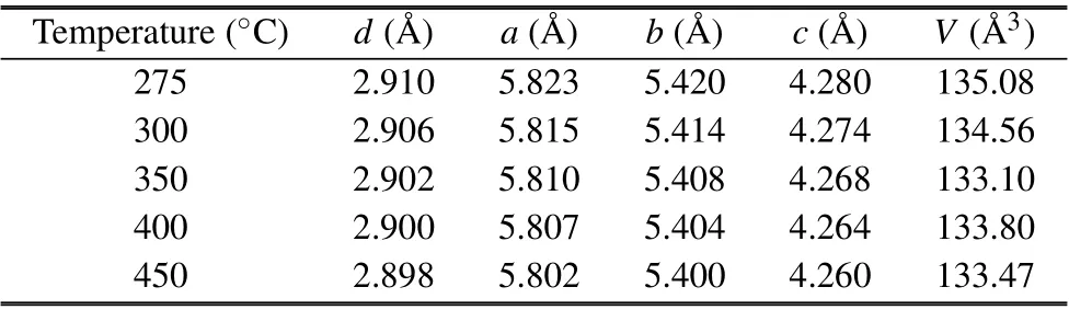
Table 1.The crystallographic plane spacing,estimated lattice constants,and unit cell volumes of the samples synthesized at different temperatures.
2.2. Structural characterization and absorption measurements
The XRD patterns of the samples were recorded with a Bruker D8 Advance diffractometer using Cu Kα (λ =1.5418 ˚A) radiation and which was operated at 40 kV and 40 mA.The spectra were collected in the range 2θ =10◦–80◦with a scanning rate of 2◦per minute. The crystal morphology and average crystallite sizes of the samples were determined from high-resolution transmission electron microscopic(HRTEM) images. The microscope used (FEI Model Tecnai S-twin) had a resolution of 0.24 nm. Small amounts of the nanoparticulate samples were dissolved in absolute ethanol and homogenized with the help of an ultrasonicator. The UV–Vis spectra absorption measurements were carried out at room temperature using a Shimadzu, UV-1800 double-beam spectrophotometer. Infrared spectra were taken from a Perkin Elmer Frontier FT-IR spectrometer and using KBr pellets as the matrix.
2.3. Positron annihilation measurements
Positron lifetime measurement was performed employing barium fluoride(BaF2)scintillators coupled to XP2020Q photomultiplier tubes using a 10µCi strong22Na radioactive isotope as the source of positrons. The source material was basically in the form22NaCl dissolved in dilute HCl acid,and the source for the experiments was prepared by the deposition of the solution on a very thin (~2 mg/cm2) and well-annealed Ni foil. The extended portion of the foil was folded to cover the source deposition. The source in this form was kept at the geometrical center of the column of the powdered sample taken in a glass tube of length 14 cm and cross-sectional area 0.785 cm2. The glass tube was continuously evacuated during the data acquisition to remove the traces of air that may get otherwise trapped in the powdered column of the sample,and the powder was able to settle down under its own weight.Thus, the sample and the source had always been kept in moisture-free conditions. The sample covered the source from all sides abundantly to ensure positron annihilation within it,and no positrons reached the walls of the glass tube as the radius of the tube is 0.5 cm. The positron lifetime spectra were recorded using a standard slow-fast gamma-gamma coincidence setup with a time resolution of 0.200 ns(full width at half maximum). For coincidence Doppler broadening spectroscopic(CDBS)measurements,two high purity germanium semiconductor(HPGe)detectors were used,which had energy resolution 1.27 and 1.33 keV at 0.511 MeV, i.e., the positron annihilation gamma-ray energy. Sufficiently large numbers of counts(~3×10⁶)were collected under each positron lifetime spectrum. In CDBS measurements,about 2×10⁷coincidence events for as long as 44 hours were generated under the twoparameter spectra described later. To determine the S and W parameters from CDBS spectra the energy span of E1+E2=1.022±0.00145 MeV along the direction ∆E =E1−E2was chosen.
3. Result and discussion
3.1. XRD studies
The XRD spectra of the samples, shown in Fig.1, consisted of diffraction peaks in good agreement with those reported in JCPDS card No.77-1971, and the observation confirmed the purity and single-phase nature of the samples. All the samples showed the main peaks corresponding to the(100), (111), (200), (020), (002), (300), and (222) planes of orthorhombic structure. The lattice constants of the samples were estimated from the XRD data by relating the Bragg’s equation[32]with the spacing of the crystallographic planes(d)as

The values of lattice constants(a,b,and c)are calculated for all the samples and are in good agreement with the standard data. The calculated lattice constants of the unit cells and the volume(V =abc)of the unit cells corresponding to the sample treatment temperatures are given in Table 1. The average crystallite sizes(D)of the different samples were estimated by using the Debye–Scherrer equation[33]
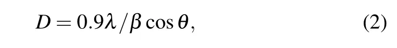
where λ is the wavelength used for Cu Kα radiation and β is the full width at half maximum(FWHM)of the diffraction peak at an angle θ. We used the most intense peak (111) in the XRD pattern to determine the average crystallite size. The average crystallite sizes of the samples are varied from 20 nm to 35 nm. Table 2 shows the details of the sample treatment temperature,annealing time,and the obtained crystallite sizes.
Table 2. The sample treatment temperature, annealing time, and the obtained crystallite sizes.
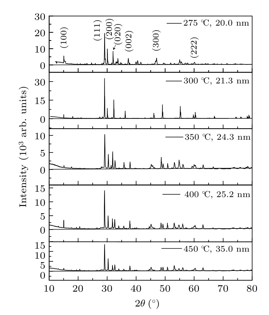
Fig.1. XRD patterns of the PbO nanocrystalline samples.
Figure 2 shows the variation of the volume of the unit cells with the crystallite size. A lattice expansion with decreasing crystallite size is evident from these results. It has been proposed by Manuel Diehm et al.[34]that the increase of the lattice constants of metal oxides with decreasing crystallite size can be caused either by the presence of excess vacancy type defects or by a negative surface stress, and exact identification of either of them as the true cause is difficult due to their simultaneous occurrences and dominating nature at similar crystallite size ranges in typical metal oxides.[34]
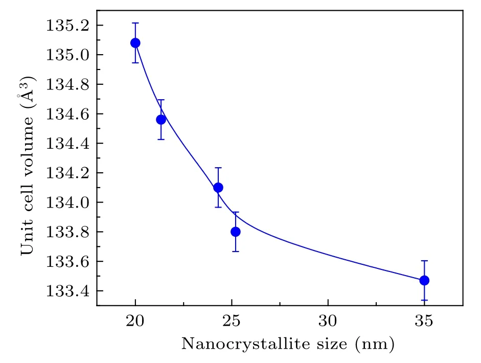
Fig.2. The unit cell volume versus the average crystallite size of the samples.
3.2. HRTEM analysis
The HRTEM images of some of the PbO samples are shown in Fig.3.Figures 3(a)–3(c))show that the samples consist of PbO nanocrystals with sizes of 21 nm, 25 nm, and 35 nm. The well-developed lattice fringes shown in Figs. 3(d)–3(f)are proof of the high degree of crystallinity of the samples.The crystallite sizes are confined to a very narrow distribution,and they are uniform in shape and size. The HRTEM images also support the XRD results in terms of the nanocrystallite sizes,which show that the nanocrystallite sizes of the synthesized samples are larger and uniformly distributed at higher temperatures.
3.3. Optical absorption measurements
UV–Vis light absorption spectroscopy is an important method to show the optical properties and energy structure of nanocrystalline samples.The optical absorption spectra for the nanocrystalline samples are presented in the range from 200 to 800 nm in Fig.4. It is clear that in the region 230 to 800 nm,the absorption peaks gradually decrease with the increase of the wavelength.
The optical band gap(Eg)was calculated from the optical absorption spectra using the Tauc’s relation αhν = A(hν −Eg)n, where hν is the photon energy, A is a constant, and n depends on the nature of the transition.[35]The value of n is 1/2 for direct transitions and 2 for indirect transitions. Since PbO is well known as a direct band semiconductor,[36]the optical band gap[37]for the synthesized samples are obtained by extrapolating the linear part of the (αhν)2against hν curve to zero on the y-axis. The band gap energies of the PbO nanocrystallites are in the range of 2.97–2.34 eV(Fig.5).

Fig.3.HRTEM images of some of the PbO nanocrystalline samples:(a)–(c)the nanocrystalline particles,(d)–(f)the well-developed lattice fringes.
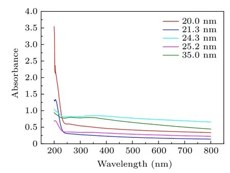
Fig.4. UV-Vis absorption spectra of the different samples.
Typically, nanocrystallites show a blue shift in the band gap energy as the crystallite size decreases. In this case, we also observe that the edge of the absorption shifts towards the lower wavelength (blue) region of the spectrum. Therefore,the band gap increases as the crystallite size decreases(Fig.5).The value of Egand its changes with crystallite sizes are identical in nature and magnitude to the changes expected in the event of quantum confinement effects,which are expected and have been observed in certain other nanocrystalline systems earlier.[38–41]For example,the exciton Bohr radius in the case of PbS nanocrystallites is 18 nm,[42]which means the band gap energies[43,44]would show a definite increase in crystallites of sizes 36 nm and below. Assuming that a similar value holds good for PbO nanocrystallites,the present results agree with the onset of similar effects.
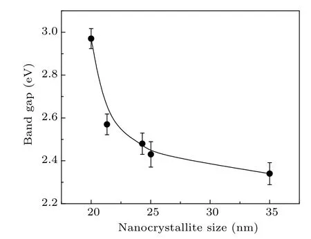
Fig.5. The band gap estimated from the optical absorption spectra versus the size of the nanocrystallites of the samples.
3.4. FT-IR studies
Figure 6 shows the FT-IR spectra of the PbO nanocrystalline sample synthesized at 350◦C. The absorption peak around 461 cm−1in PbO is related to the vibration of Pb–O bonds. The bands at 927.3 cm−1and 1049.3 cm−1of very low intensities are attributed to oxygen stretching[45]and bending frequencies. The robust and intense peak at 1410.4 cm−1is due to the –OH deformation vibration of the H2O molecule.The broad band with very low intensity at 3444.3 cm−1is associated with the stretching vibration of the hydroxyl (OH)group, and it is due to little amounts of H2O being absorbed on the surfaces of PbO nanostructures.[46,47]
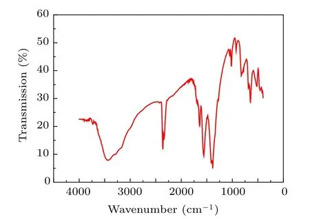
Fig.6. FT-IR spectra of the nanocrystallitine sample synthesized at 350 ◦C.
3.5. Positron lifetime measurements

Fig.7. The variation in(a)the positron lifetimes and(b)the relative intensities versus sample synthesis temperatures.
The detailed analysis of the positron lifetime spectra is carried out using the PALSfit program.[48]The analysis gave the best fit for three lifetime components,which are named τ1,τ2, and τ3in the ascending order of magnitudes. The corresponding relative intensities are named as I1, I2, and I3irrespective of their magnitudes. The variations of the positron lifetimes and their intensities versus the sample synthesis temperatures, as depicted in Figs. 7(a) and 7(b), are crucial in understanding the evolution of the defects under crystallite growth.
The shortest positron lifetime τ1signifies the annihilations of positrons in free states. This refers to those positrons which, during the time of their diffusion through the crystallite,come into random physical contact with the electrons and get annihilated instantaneously. The longest lifetime τ3, the magnitudes of which are spread over a few nanoseconds,is not generally expected in high electron density solids like metal oxides. This lifetime component is related to the formation and subsequent annihilation of ortho-positronium atoms (o-Ps), a metastable spin-triplet-bound state of the electron and positron (where both spins are parallel), and which is generally formed in sites of very low electron density. Here, in this case, since the materials are nanocrystalline in compositions, there is a large network of surfaces and intercrystallite interfaces. These are low electron density sites in which positron gets highly localized and can form its metastable bound state known as positronium. When formed, the parapositronium state(the spin singlet where electron and positron spins are aligned anti-parallel) gets less populated than the spin triplet state counterpart called ortho-positronium, where both the electron and the positron have spins aligned parallel. In fact, the ratio of formation of the two states is 1:3.So, a small contribution coming from para-positronium with a lifetime of 0.125 ns will also be there in τ1. Since the intensity I3itself is very small (i.e., less than 1%), the parapositronium contribution to τ1can be ignored. The component that is specifically interesting to defect identification and analysis is τ2and its intensity I2. Normally this comes from positron trapping in vacancy type defects arising from lack of occupancy of some of the lattice sites by the respective atoms or ions due to thermodynamic conditions.Defects are inherent aspects of solid-state systems in general, and attaining a perfect stoichiometry is almost impossible. The concentrations of defects are normally below the sensitivity of conventional techniques like XRD, SEM, and TEM. Positron annihilation,on the other hand,is most sensitive to detect the structural defects in solids,even at the atomic level. The values of τ2and I2,therefore,can be attributed to positron trapping and annihilation in the non-stoichiometric defects.
Since the material used here are nanocrystalline, and the positrons normally can diffuse driven by the thermal energy over distances about 50–100 nm, there is an additional lifetime component merging with the defect component. This comes from the positrons diffusing out and getting annihilated from the nanocrystallite surfaces. Hence the values of τ2and I2are more than what are normally expected for positron annihilation in crystal defects. Within the limitations of the instrumental resolution, it is not possible to separate it out.However, although the surface contribution is significant, it changes its value only when the nanocystallite sizes become less than about 10 nm. Since the nanocrystallites in this work are larger than this limit, the variations of τ2and I2are assigned to the vacancy type defects in the samples rather than the change in nanocrystallite surface properties.
The variation of the defect-specific positron lifetime τ2is illustrated in Fig.7. It shows that vacancies agglomerate to form large vacancy clusters. The electron density seen by the positrons drastically reduces with an increase in the volume of defects that trap positrons. In this case, however, the values of τ2in the range of 0.35 to 0.37 ns are rather large compared to the positron lifetimes in typical vacancy type defects, which may lie in between about 0.2 to 0.3 ns.[49]The larger values of τ2have a special significance due to the nanocrystallinity of the samples. An appreciable percentage of positrons, which are already thermalized due to multiple energy dissipative processes in the material, will diffuse out to the surfaces of the nanocrystallites.[49,50]Since surfaces are low electron density sites, the positron lifetimes are expected to be large, but it gets admixed with the vacancy type defects component. In other words, τ2contains contributions from both defects as well as surfaces. The corresponding intensity I2, in the meanwhile, decreases first, indicating that the defect concentration decreases. This suggests that vacancy type defects agglomerate, their sizes increase and their number decreases. The ortho-positronium lifetime τ3and its intensity I3also show similar trends. The increase of the shorter lifetime τ1and its intensity I1also indicates that the defect concentration decreases in samples when synthesized at higher temperatures. The mean positron lifetime (τm) is defined as

Figure 7 shows that for the first two components of the lifetime, the variations of corresponding intensities are in the opposite direction. Net τmdecreases with an increase in temperature.When a positron annihilates with an electron inside a defect,the lifetime increases if the defect size becomes larger,and intensity decreases if defect concentration decreases. The behavior of the mean positron lifetime (τm) and the positron lifetime in bulk PbO (τb), which is calculated from the relation

in Fig.8,also suggests that defect concentration is less and the sizes are larger in the samples synthesized at higher temperatures.

Fig.8. (a) The mean positron lifetime (τm) and (b) the bulk positron lifetime(τb)versus annealing temperatures of the PbO nanoparticles.
3.6. Coincidence Doppler broadening measurements
The CDBS spectra were analyzed by generating ratio curves of events with respect to pure and well annealed aluminum (Al) single crystalline sample.[51]The results are shown in Fig.9. The ratio curves are usually generated with respect to the identically acquired spectrum of a reference sample,a pair of sintered Pb pellets here. With Pb as the reference, we found the peaks shifted to 11×10−3m0c. This is justified as the ratio curve of Pb with respect to Al,which has a distinct local minimum at 10.75×10⁻³m0c that can be seen in the inset of Fig.9. The peak at pL=10×10−3m0c is due to positron annihilation with the electrons in the 2p orbital of oxygen ions.[40]The curves indicate reduced annihilation in defects in samples prepared at 400◦C and 450◦C.It supports the findings of the positron lifetime measurements and is more vividly displayed by the variations of the S and W line-shape parameters. These parameters are respectively estimated as the ratio of events under ∆E=±0.00058 MeV and jointly under ∆E =±0.00203 to ±0.00319 MeV of the projected onedimensional spectra to the total events under it. Measured as this,the two parameters are defined as the fraction of low(valence)and high(core)momentum electrons annihilated by the positrons. S parameter is calculated from the central region of DBS spectra, and W parameter is calculated from the wings region of both sides of these spectra. In order to understand the evolution of the defects under the growth of the nanocrystallites, the variations of the S and W parameters are shown against the synthesis temperature of the nanocrystalline samples in Fig.10.
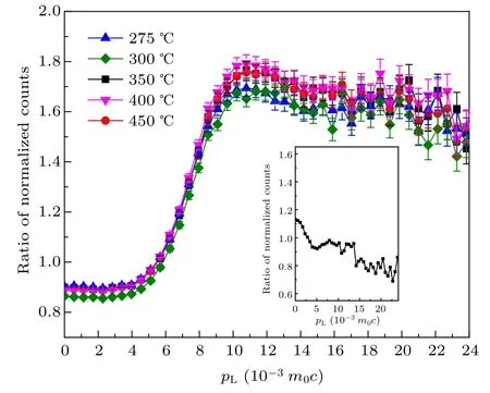
Fig.9. CDBS ratio curves of a few selected samples with respect to that of an identical curve for pure and annealed Al pellets. The inset figure contains the CDBS ratio curve of Al pellets.

Fig.10. The(a)S and(b)W parameters versus the synthesis temperature of the samples.
Qualitative changes in the S and W values often indicate the defect evolution processes undergoing within the samples at the atomic scale.The sharp fall of the S parameter till 400◦C of the prepared samples is indicative of the defects agglomeration taking place on a larger scale. Since the nanocrystallite sizes also increase, the fraction of positrons reaching the surfaces of the crystallites decreases. However, the final rise of the S parameter in the sample prepared at 450◦C could not be explained at this stage,although repeated measurements confirmed the results.The behavior of the W parameter is complementary to the variation of the S parameter,as expected. The S–W plot is shown in Fig.11.The results indicate that positron annihilation parameters are helpful in indicating the evolution behavior of defects in metal oxide nano-systems, which will have significant effects on their optical, electrical, and magnetic properties.
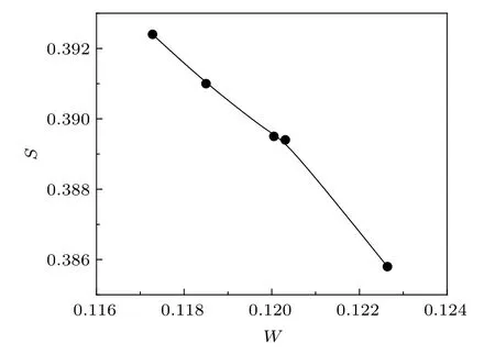
Fig.11. The S–W plot.
4. Conclusions
In this work,PbO nanocrystalline samples have been synthesized by the sol-gel method at different temperatures to vary the nanocrystallite sizes.The XRD analysis shows the orthorhombic structure of PbO,and the average particle sizes of synthesized PbO are in the range of 20–35 nm.HRTEM analysis confirmed that the samples had been synthesized to evolve in a highly pure composition, and the sizes of the nanocrystallites could be confined to a very narrow distribution. The band gap energies of the PbO nanoparticles are in the range of 2.34–2.97 eV.The investigation to study their optical properties revealed a significant increase in the band gap energy with a decrease in particle size that notified the occurrence of quantum confinement effects. The FT-IR spectra of the samples showed an absorption peak corresponding to the vibration of Pb–O bonds and a broad band of very low intensity due to the stretching vibration of the OH group. Bands of very low intensities attributable to oxygen stretching and bending frequencies could also be identified.Positron annihilation studies were carried out to verify the presence of vacancy type defects in the samples,and the defects grew into large vacancy clusters when the synthesis temperatures were increased.
One of the most important applications[52]of the lead oxide nanoparticles is that it can be used as cathode and anode electroactive material in lead acid batteries. The anodes and cathodes made by PbO nanoparticles show excellent discharge capacity and cycle life.[53]The discharge capacity of batteries is enhanced while using nanoparticles of PbO,and the use of nanoparticles[54]in the paste of electrodes reduces the discharge resistance by 50%. It can cause the delivery of more power to an external load. More than 130 Ω/g discharge resistance density can be obtained when using PbO nanoparticles instead of bulk PbO.We have also prepared the nanoparticles by a more convenient and economical sol-gel route of crystallite sizes of the same dimension. A wide range of nanoparticles have been synthesized,and further research is being carried out to look at how nanocrystallite size affects the discharge rate.
Acknowledgements
Sk Irsad Ali gratefully acknowledges The University of Burdwan for granting the state-funded fellowship. The authors wish to thank Dr. Goutam Das of National Metallurgical Laboratory,Jamshedpur,India,for providing the facilities for HRTEM images. The authors also acknowledge Prof. P. K.Chakrabarti and Prof P. Mitra, Department of Physics, University of Burdwan, and Prof. A. K. Ghosh, Department of Chemistry,University of Burdwan,for providing instrumental facilities for the synthesis of the samples.
杂志排行

Chinese Physics B的其它文章
- Novel traveling wave solutions and stability analysis of perturbed Kaup–Newell Schr¨odinger dynamical model and its applications∗
- A local refinement purely meshless scheme for time fractional nonlinear Schr¨odinger equation in irregular geometry region∗
- Coherent-driving-assisted quantum speedup in Markovian channels∗
- Quantifying entanglement in terms of an operational way∗
- Tunable ponderomotive squeezing in an optomechanical system with two coupled resonators∗
- State transfer on two-fold Cayley trees via quantum walks∗