用于流水线ADC的无采样保持运放前端电路
2020-11-09陈迪平张仁梓曹伦武陈卓俊曾健平
陈迪平 张仁梓 曹伦武 陈卓俊 曾健平

摘 要:为了降低流水线模数转换器功耗与提升输入信号范围,设计了一种无采样保持运放前端电路. 移除采样保持运放降低了功耗,并改进开关时序进一步降低电路功耗;同时改进传统开关电容比较器输入,使得模数转换器可达到0 ~ 3.3 V满电源电压的量化范围. 将设计的无采样保持运放前端电路应用在一款低功耗12位50 MS/s流水线模数转换器进行验证,采用0.18 μm 1P6M工艺进行流片,芯片面积为1.95 mm2. 测试结果表明:3.3 V电压下,采样率为50 MS/s、输入信号频率为5.03 MHz时,信噪失真比(SNDR)为64.67 dB,无杂散动态范围(SFDR)为72.9 dB,功耗为65 mW.
关键词:流水线模数转换器;无采样保持运放;孔径误差;开关电容比较器
中图分类号:TN495 文献标志码:A
Front-end Circuit without Sample-and-hold
Amplifier for Pipelined ADC
CHEN Diping1,ZHANG Renzi1?,CAO Lunwu2,CHEN Zhuojun1,ZENG Jianping1
(1. College of Physics and Microelectronics Science,Hunan University,Changsha 410082,China;
2. Hunan Advancechip Electronic Technology Company,Changsha 410205,China)
Abstract:A front-end circuit without Sample-and-Hold Amplifier(SHA) is presented for reducing power consumption and increasing input range of pipelined ADC. Removing Sample-and-Hold Amplifier and improving switching timing reduce the circuit power consumption,while improving the traditional switched-capacitor comparator inputs to make ADC achieve a 0-3.3V full supply voltage quantization range. The front-end circuit without Sample-and Hold Amplifier is verified in a low power 12 bit 50 MS/s pipelined ADC. The circuit is implemented in a 0.18 μm 1P6M process,and occupies a chip area of 1.95 mm2. The test results with a 5.03 MHz input wave under a sampling rate of 50 MS/s show that the ADC achieves a 64.67 dB signal-to-noise and distortion ratio(SNDR) as well as a 72.9 dB spurious-free dynamic range(SFDR),while it consumes the power consumption of 65 mW.
Key words:pipelined Analog to Digital Converter(ADC);Sample-and-Hold Amplifier(SHA)-less;aperture error;switched-capacitor comparator
高速高精度模數转换器(Analog to Digital Converter,ADC)是如今众多高性能数模混合电路系统中不可或缺的部分[1-4].随着工艺水平的提高以及便携式电子设备的兴起,高速低功耗ADC[5-6]也正成为研究热点. 常见的ADC有流水线型(Pipelined)[7-8]、逐次比较型(Successive Approximation Register,SAR)[9]、混合型(Pipelined-SAR)[10]、过采样型(Sigma Delta,Δ-Σ)[11]等,而Pipelined ADC因其较快的速度、较高的精度以及适中的功耗而被广泛应用.
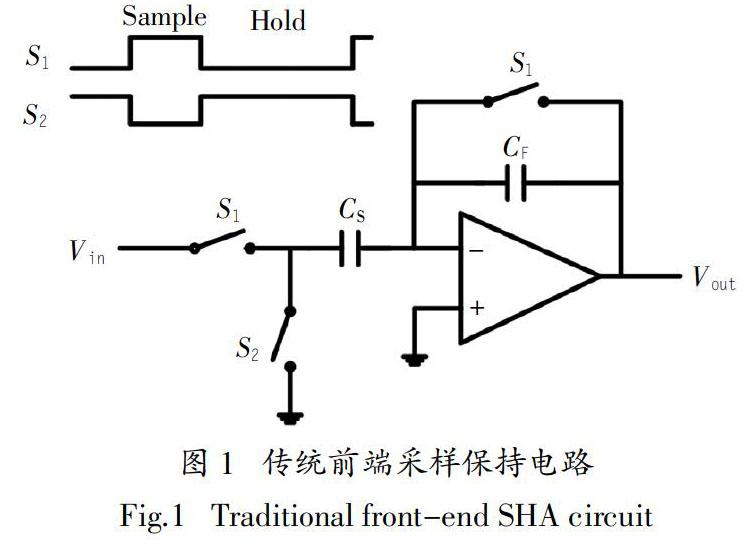
为达到低功耗Pipelined ADC设计要求,研究者们提出了许多降低功耗方法,如运放共享技术[12]、无前端采样保持运放技术(Sample-and-Hold Amplifier-less,SHA-less)[13-14]等. 传统Pipelined ADC设计中,为使子ADC和余量增益电路(Multiplying Digital-to-Analog Converter,MDAC)两条路径传输信号一致,信号通过采样保持电路(Sample-and-Hold Amplifier,SHA)后才开始逐级量化. 由于SHA电路位于ADC最前端,为达到高速高精度目的,系统对SHA中运放的增益与带宽具有很高要求,从而消耗巨大功耗. 因此,降低Pipelined ADC功耗的……