基于FPGA的OOK可见光通信系统仿真与实现
2020-09-21王许浦孙晓红薛琦
王许浦 孙晓红 薛琦
摘 要: 根据OOK(开关键控)的原理,基于FPGA开发板用Verilog HDL语言实现OOK调制、解调和同步模块,并通过逻辑分析仪进行仿真。配合驱动电路、光电探测电路和放大电路等实现了整套可见光通信系统的设计,最后通过搭建实验平台进行测试,测试结果表明,收发电路通信距离达到12 cm,系统传输速率达到3.125 Mb/s。
关键词: 可见光通信; FPGA; OOK; 驱动电路; 光电探测器; 位同步
中图分类号: TN929.1?34 文献标识码: A 文章编号: 1004?373X(2020)17?0025?04
Abstract: According to the principle of OOK (on?off keying), the modules of modulation, demodulation and synchronization are realized by using Verilog HDL language and FPGA board, and simulated by logic analyzer. The whole set of visible light communication system is designed with driving circuit, photoelectric detection circuit and amplification circuit. The experiment platform was built to test the system. The test result shows that the communication distance of the transceiving circuit can reach 12 cm, and the transmission rate can reach 3.125 Mb/s.
Keywords: visible light communication; FPGA; OOK; drive circuit; photo detector; bit synchronization
0 引 言
可见光通信技术可以解决传统无线通信存在频谱资源紧缺、信息不安全以及电磁干扰等问题,同时,它在高速通信的同时又具备节能照明的特点而被广泛关注和研究[1?3]。目前研究可见光通信的很多,但是基于FPGA的可见光通信系统研究还并不多,由于FPGA具备运行速度快、管脚多和设计灵活等优点,因此,将可见光通信技术与FPGA相结合可以大大提高系统的性能[4?5]。本文基于FPGA开发板,运用Verilog HDL语言并结合电路设计搭建起一套可见光通信系统并进行验证。
1 可见光通信系统整体设计
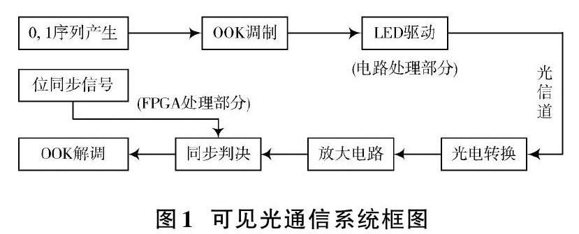
本系统发射端采用Alter公司Cyclone系列芯片,型号为EP4CE15F23C8的FPGA开发板对信号进行数字处理及时序控制,接收端采用Alter公司Cyclone系列芯片,型号为EP4CE30F23C8的FPGA开发板对接收的信号进行处理。重点在于OOK(On?Off Keying)的调制解调、同步等算法与Verilog HDL语言实现,以及发送电路设计和接收电路中互阻放大电路、同相积分器等电路的设计。其中,系统发射端的信号为FPGA产生的0,1周期符号序列,通过OOK调制到白光LED驱动电路中;系统接收端包括光电转换模块、放大电路模块和FPGA解调模块等,如图1所示。……
