Theoretical Model and Suppressing Method of Interface Charge Accumulation in HVDC Cable Accessory: A Review
2020-01-07LIJinHANChenleiLIZhijianDUBoxueTatsuoTakada
LI Jin, HAN Chenlei, LI Zhijian, DU Boxue, Tatsuo Takada
(1.School of Electrical and Information Engineering, Tianjin University, Tianjin 300072, China; 2.Electric Power Research Institute of State Grid Tianjin Electric Power Company, Tianjin 300084, China; 3.Tokyo City University, Tokyo 158-8557, Japan)
Abstract: HVDC cable has been widely used with the development of flexible HVDC transmission. Cable accessories are the weakest part of HVDC cables, while the most serious problem of DC cable joint is the uneven distribution of electric field caused by space charge accumulation, which may lead to the ageing and failure of joint insulation, especially at the interface between different materials. In this paper, the progress of the interface charge research of the HVDC cable accessories is discussed, the existing theoretical model and the suppression method of the interface charge are analysed, and the research trend of the interface charge of the accessories in the future is prospected. The results show that space charges accumulate at the interface between different material are closely related to temperature, applied electric field and working conditions such as polarity reversal, etc.; the Maxwell-Wagners-Sillars theory and bipolar charge transport model are discussed in detail, and the method of using quantum chemical theory to calculate and analyse interface charges is introduced; the methods of interface charge suppression based on geometry design, surface modification, field grading materials and material selection are analysed and compared. The summary and conclusion of these research results can provide reference for the future research on the interface charge behaviours and suppression methods of HVDC cable accessories.
Key words: HVDC cable accessory; interface charge; transportation model; suppressing method; quantum chemical calculation
1 Introduction
The innovation in technology of next-generation power electronics promotes the development of large-scale energy transmission by high voltage direct current (HVDC), which interconnects networks composed of renewable energy sources with main power grids or regions of consumption[1-3]. Particularly, as the major equipment in HVDC transmission network, HVDC cable has been one of the best options for long-distance large-capacity transmission and urban power supply, which expanded the application range of polymeric insulated cables considering the great advantages of their lower losses and unique practical feasibility[4]. The insulation properties of cable accessories are vital for the safe operation of HVDC cable transmission networks, as well as for the responsibility of HVDC transmission systems[5-7].
It is generally known that the electric field distribution under AC conditions isbasically capacitive and depends on the permittivity reciprocal of material, which is insensitive to electric field or ambient temperature[8]. However, the distribution becomes resistive under DC conditions, while conductivity is drastically dependent on temperature and exhibits nonlinear characteristics in high electrical field[9-10]. Figure 1 exhibits the schematic cross section of an HVDC cable joint. Under the condition of a DC electric field, the space charge at the interface between dielectrics is likely to accumulate because of the various characteristics of different dielectric materials, and this accumulation may accelerate the degradation of HVDC cable accessory systems under combined stresses[11-12]. The complex geometry and doping of fillers coupled with nonlinear effects render the interface charge performance difficult to evaluate in operation[13]. To alleviate this problem, it is necessary to establish an accurate theoretical model for evaluating the interface charge behaviour of HVDC cables and finding the charge accumulation suppression methods, which is of great significance for insulation design of HVDC cable accessories[14]. In this paper, interface charge behaviours together with Maxwell-Wagners-Sillars (MWS) theory, bipolar charge transport model, quantum chemical model and some suppression methods will be reviewed to better understand and regulate the interface charge behaviours in HVDC cable accessories.

Fig.1 Cross-sectional view of an HVDC cable joint
2 Interface Charge Accumulation
2.1 Space Charge Characteristics in Double-Layer Dielectrics
The double-layer dielectric structure composed of polyethylene and rubber is a classical design of accessories for HVDC cables[6]. A typical interface charge distribution in EPDM/LDPE double-layer dielectrics measured by using the PEA method under electric fields ranging from 10 to 60 kV/mm is shown in Figure 2. Negative charge accumulates at the EPDM/LDPE interface under a positive electric field (Figure 2a) above 30 kV/mm (shown in blue, ②). In the LDPE component, positive charge drifts to the cathode under the external electrical stress (shown in yellow, ①), while negative charge remains at the interface. In addition, under negative polarity electric fields (Figure 2b) of 20 kV/mm and above, positive charge distributes at the anode and interface (shown in yellow, ③ and ④).
2.2 Interface charge characteristics under voltage polarity reversal
Space charge tends to accumulate at the interface between materials as shown above. Accordingly, polarity reversal, which occurs occasionally in HVDC cable systems, is extremely important as the electric field in the space charge region will become more instantaneously, which may worsen the insulation and even lead to its breakdown[8]. Space charge behaviours in EPDM/LDPE samples at 40 kV/mm before and after voltage reversal are shown in Figure 3a, while Figure 3b shows the temporal variation of the maximum electric field intensity of EPDM and LDPE after 30 minutes of poling for each series voltage reversal[6].

Fig.2 Space charge distribution in an EPDM/LDPE double-layer structure under various applied electric fields
Obviously, regardless of the polarity of applied voltage, the maximum electric field on the EPDM side occurs over time.
As shown in the figures, the space charge behaviours in double-layer media exhibit four important characteristics as follows:
1) Positive chargeis generated at the interface and move faster in the medium than the negative charge generated at the cathode (Figure 3a, ①).
2) The negative charge generated at the interface is trapped on the side of EPDM and has difficultyin migrating (Figure 3a, ②).
3) The positive charge injected from the anode is packet-like and drifts rapidly to the interface (Figure 3a,③).
4) The injected positive charge accumulates at the interface and is trapped on the side of the EPDM again (Figure 3a,④).
3 Theoretical Models of Interface Charge
3.1 Maxwell-Wagners-Sillars Theory
Maxwell-Wagners-Sillars (MWS) theory, as the most common mechanism for explaining interface charge accumulation along with the stress time, takes interfacial polarization as the core[15]. Concretely, HVDC cable accessory is simplified into a dual-layer model consisting of two dielectrics, as shown in Figure 4, where +Uis the external applied DC voltage, andΣsis the space charge density at the interface.

Fig.3 Space charge distribution and maximum electric field in EPDM and LDPE layers under voltage polarity reversal
According to the Maxwell equations:
σ1E1=σ2E2;
(1)
d1E1+d2E2=-U;
(2)
ε1E1-ε2E2=Σs.
(3)
whered1andd2are the thickness of dielectric 1 and 2,ε1andε2are the permittivity andσ1andσ2are the conductivity. Then,Σsthe interface charge density of the dual-layer dielectrics with differentialεandσcan be expressed by equations (4) and (5):
(4)
(5)
wheretcis the characteristic time depending on the physical size and dielectric properties of the two materials[16]. It can be speculated from equation (4) that more space charges will be produced with more serious mismatch in the conductivity and permittivity between the two dielectric materials, and the interface charge build-up procedure is determined by the time constanttc. In other words, the polarity and quantity of interface charge are functions of electrical field and ambient temperature, which can be calculated from the measured permittivity and conductivity values using the MWS theory.

Fig.4 Interfacial polarization in the dual-layer dielectrics according to the Maxwell-Wagner-Sillars model
According to the measured conductivity andMWS theory, Vuetalpredicted the functional relationship between the quantity of interfacial charges in double-layer XLPE/rubber media and the applied voltage and temperature in a DC electric field[15]. Figure 5 illustrates the relationship between the polarity of the calculated interface charge and temperature and the average applied electric field under steady-state conditions.
For electric fields ranging from 2 to 22 kV/mm and temperatures from 0 to 86 ℃, there are two distinct positive and negative charge regions at the interface between the two dielectrics, separated by the dependence demarcation line of temperature and electric field.

Fig.5 Predicted landscape for the sign of the interfacial charge for the dual-layer system of a cable accessory
3.2 Bipolar Charge Transport Model
Figure 6 shows the mechanism of bipolar charge transportation in a dielectric. It is obtained based on the calculation shown below.
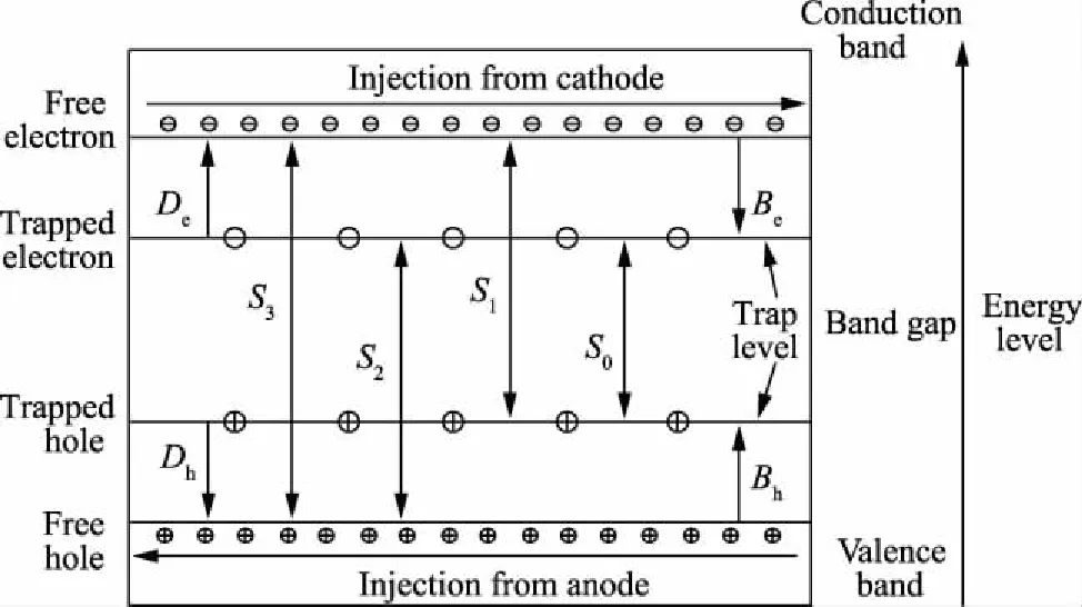
Fig.6 Mechanism of bipolar charge transportation in a dielectric
In solid dielectrics, carriers are governed by a set of self-consistent equations as follows[17-18]:
·Current continuity equation:

(6)

(7)
(8)
(9)
whereqf-andqf+are the charge densities of the mobile negative and positive carriers, C/m3;qt-andqt+are the charge densities of the trapped negative and positive carriers, C/m3; andj-andj+are the conduction current densities of the mobile negative and positive carriers, A/m2. The charge trapping-detrapping and recombination processes are considered in the following source terms, wheresf-andsf+are the source terms of the mobile negative and positive carriers, C/(m3·s); andst-andst+are the source terms of the trapped negative and positive carriers, C/(m3·s).
(10)
(11)
(12)
(13)
whereQt-andQt+are the trap densities, C/m3;PtrandPdeare the charge trapping and detrapping coefficients, 1/s; andRis the recombination coefficient, m3/(C·s)
·Charge transport equation:

(14)

(15)
whereμ-andμ+are the mobility of negative and positive carriers, m2/(V·s);D-andD+are the diffusion coefficients of negative and positive carriers, m2/s; andEis the electric field strength, V/m.
·Poisson’s equation:
(16)
E=-U.
(17)
whereUis the electric potential, V;ε0is the permittivity of vacuum, F/m; andεris the relative permittivity of the dielectric.
·Boundary conditions:
At the boundaries between the dielectric and the metal electrodes, the normal current densities can be described as:
(18)
(19)
whereα= 1 at the cathode andα= 0 at the anode; andJs-andJs+are the Schottky injection current densities, which can be described as follows:
(20)
whereAis the Richardson constant, C/(m2·s·K2);φis the contact potential barrier between the dielectric and the metal electrode, eV;kBis the Boltzmann constant; andTis the thermal temperature, K.
The simulation results show that the interface charge density in the HVDC cable accessory is increased by the deep surface trap energy level, high interface barrier and large carrier mobility difference[19]. The accumulation of interface charge causes distortions in the electrical field distribution.
3.3 Interface charge model based on quantum chemical calculations
The Gaussian 09 quantum chemical program can be used to calculate the energy bands of LDPE and EPDM, while B3LYP was chosen as the exchange correlation function and 6-31 G* was chosen as the basis set[20-21]. To assist in the analysis of the complex space charge behaviour observed at the interface between the two dielectrics, the electronic energy levels of the double-layer EPDM/LDPE system are calculated[6]. The calculated electronic energy levels in Figure 7 are obtained in the case of electrode contact. The results show that when EPDM and LDPE are in contact, the dielectric system will polarize and be exposed to voltage reversal. In the absence of applied voltage, considering that the Fermi level of LDPE (Ef=-3.0 eV) is lower than that of EPDM (Ef=-2.6 eV), positive charges will accumulate on the side of LDPE (Figure 7b ③), and negative charges will accumulate on the side of EPDM (Figure 7b ④). In Figure 7a, the electronic energy levels of the double dielectrics are shown when the positive voltage is applied to the SC electrode. Positive charges can drift more easily through shallow traps in LDPE. However, negative charges in the double-layer dielectrics can be trapped in deep traps on the surface of EPDM (Figure 7a ②, electron trap depthφte= 0.9 eV-1.1 eV), so it is not easy for them to drift through EDPM.

Fig.7 Energy levels within the double-layer LDPE/EPDM system with different voltage application
The polarity of the injected interface charge is consistent with that of the voltage applied on the LDPE side. Compared with the negative charge, the polarity of injected charge is dominated by the positive charge. The difference in the distribution of holes and electron traps leads to polar-dependent charge motion, which is determined by means of QCC (quantum chemical calculations). Deep traps in EPDM materials are the main reason for the accumulation of interfacial charges on the LDPE side. With the reversal of the applied voltage, the residual interfacial charge at the interface is neutralized by the heteropolar charge injected from the LDPE side. After that, additional injected charge will be trapped at the interface.
4 SuppressionMethods
Interface chargebehaviours are rather complex, especially under various stresses, such as electrical field, ambient temperature, mechanical deformation and different contact states. Researchers developed a number of methods to suppress the accumulation of interfacial charge at the interface based on the above theories, in order to improve the reliability of HVDC cable accessories and systems.
4.1 Geometry Design
Electric field influences the interface charge characteristics greatly. Therefore, an optimized field distribution can effectively regulate the space charge injection or accumulation. A common method is to use a deflector that is made of conductive rubber to realize the field control (field-grading, FG). However, this form of “geometric” FG takes up more space and material, and it is obviously “static” even when the electric field distributions vary with time (e.g., load cycles). Therefore, it must be designed for the worst case. In this way, geometric FG can lead to over-design of the whole device, resulting in a significant increase in cost, especially for equipment used in high-pressure environments. Actually, the application of “geometry” FG in EPDM joints with voltage grades up to 320 kV has achieved satisfactory results, which is also the operating limit of current HVDC extruded cable joints (see Section 1)[22].
4.2 Surface Modification
As mentioned insections 3.2 and 3.3, an interface barrier will be induced because of the mismatch of the two materials, which includes their intrinsic surface state. Thus, a proper surface treatment could improve the contact of two dielectrics[23]. Lietaltried to modulate the surface molecular structure of EPDM and LDPE[24]. They built a gradient fluoride layer on EPDM treated with a gas mixture of N2and F2, as shown in Figure 8.

Fig.8 Comparison of the SEM and EDS of the original and fluorinated EPDM fracture surfaces
The obvious changein the cross-sectional morphology of the sample occurred after fluorination. It can be observed that fluorine (5.66 weight percent) is introduced into the surface of the sample after fluorination, which indicates that a fluoride layer with a thickness of ~2 μm was formed on the surface of the sample. For further analysis, the interface trap depth was calculated, and the results show that the modified surface state decreases the surface deep trap blocking interface charge in the HVDC cable accessory.
4.3 Field Grading Materials
Generally, when the applied DC voltage and temperature increase, the DC characteristics of different insulation materials (joints and cables) will cause unstable field distribution in the joint area of prefabricated joints.
Nonlinear resistive field grading materials (FGMs) are therefore proposed to solve the above problems[25-27]. FGMs can be obtained by adding special fillers with nonlinear conductivity to the polymer matrix under composite stress[28]. When the electric field exceeds the (critical) threshold, the conductivity of these materials can be reversibly changed from high insulation to high conductivity[25]. Therefore, for HVDC extruded cables, the latest generation of prefabricated joints may add a fourth layer of FGM (Figure 9)[28]between the internal and external deflectors. The geometry of joint insulation is designed according to the requirements of the impact test. The distribution of DC electric field is controlled by the non-linear FGM between the two layers of insulation, so that the joint is not sensitive to the change in conductivity of the two layers caused by different production and temperature.
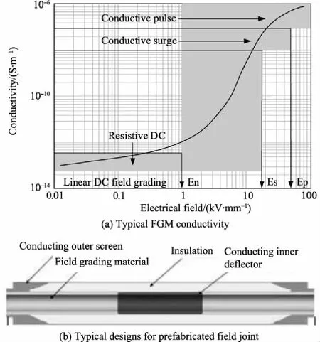
Fig.9 Typical designs for prefabricated field joints for HVDC land extruded cable systems with a field grading material (FGM) layer
4.4 Material Selection
The material properties of a joint insulation should match those of the main cable insulation, mainly in the temperature dependence of the insulation resistance. Otherwise, the electric field at the insulating interface may be distorted, which will accelerate the ageing of insulation and lead to reduction in the breakdown strength or even premature failure of insulation, especially after polarity reversal. Zhong presented a novel concept for DC cable accessory design,i.e., melded crosslinked polyethylene material has similar properties to cable insulation. Cable insulation and the enhanced insulation of accessory match well at their interface, which eliminates the interface to some extent and hence suppresses the accumulation of space charge fundamentally. Following this concept, interface-free accessories for ±200 kV DC power cables were developed and passed the test recommended by CIGRE TB 496, which verified the proposed design concept[29].
The key to the design of a prefabricated joint body lies in electric field control of the cable/joint interface and the entire medium. In the design, not only the DC voltage and different load conditions but also the switching pulses and possible lightning pulses superimposed with the DC voltage, as well as voltage interruption and voltage polarity reversal, should be considered. The tangential field of the insulation materials of the joint body and the cable under different loads should be the focus. In fact, the electric field increases seriously at the semiconductor edge at the end of the electrical grounding layer of the cable, resulting in the uneven distribution of the electric field at the junction of the high voltage cable[28]. To obtain a reasonable tangential field distribution along the interface, the temperature and electric field dependence of the conductivity of the two insulating materials must be matched[30-31].
5 Conclusions
The macroscopic parameters can be used to simulate the charge behaviour at large-scale interfaces such as cable joints and terminals to a certain extent. It must be noted that only when we know exactly how these parameters depend on the applied electric field and temperature can we use this method appropriately. In addition, once the electric field exceeds the threshold of space charge injection, the injection and extraction of charge at the electrode-polymer interface should be considered to improve the models. Among other things, the trap distribution needs to be modelled. However, to date, there is no general model to describe and explain the experimental results for dielectric interfaces.
Potential barriers and trapping sites existing in dielectric interfaces should be further investigated. In particular, the characteristics of interfacial contacts should be clarified, which are Ohmic, blocking and/or injecting in nature. The kids of carriers should be clarified.