Dynamically Tunable and High-Contrast Graphene-Based Terahertz Electro-Optic Modulator∗
2019-01-10ShaoPengLi李少鹏JingZhou周静RuiLingYin殷瑞玲andQiBingSun孙启兵
Shao-Peng Li(李少鹏), Jing Zhou(周静),Rui-Ling Yin(殷瑞玲),and Qi-Bing Sun(孙启兵)
1Department of Physics,Shanxi University of Science&Technology,Xi’an 710021,China
2State Key Laboratory of Transient Optics and Photonics Technology,Xi’an Institute of Optics and Precision Mechanics,Chinese Academy of Science(CAS),Xi’an 710119,China
Abstract We propose and discuss terahertz(THz)electro-optic modulator induced by periodically patterned graphene microcavity.Due to the joint effect of graphene plasmon resonances and Fabry-Perot(F-P)oscillations,plasmon-induced transparency(PIT)effect is achieved and the operation frequency can be dynamically tuned by graphene Fermi energies and structural parameters.The results reveal that modulation depth(MD)larger than 80%is obtained across a wide frequency range from 4.2 THz to 9.4 THz,and the largest MD and Q factor reaches 95%and 15.8,respectively.In addition,operation frequency range and MD can also be tuned by optimizing the structure parameters.This investigation promises the development of high-performance widely tunable THz modulator in chip integrated photonic circuits.
Key words:THz,modulator,graphene
1 Introduction
Electromagnetic terahertz(THz)waves which topically defined in the frequency region of 0.1 THz to 10 THz have potential for a number of applications in the research field of nondestructive imaging,[1−2]spectroscopic sensing[3−4]and ultrahigh-bit-rate wireless communication.[5−6]The past two decades has witnessed significant research development in this spectrum region.Especially the introduction and adventure of new materials such as two-dimensional semiconductor materials and metamaterials,[7−13]strong response to THz wave is not an obstacle any more.Moreover,rapid development of the quantum cascade laser(QCL)[14−15]together with high efficient THz quantum well photodetector,[16−17]promote THz technologies closer to more widespread application.However,compared with the significant advances made in THz lasers and detectors,[18−19]there is still a lack of high efficient semiconductor devices such as active filters,modulators and switches capable of manipulating THz waves.[20−22]Graphene,a monolayer of carbon atom with honeycomb structure,has attracted intense attention in the physical,chemical,and biological sciences due to its unique electronic,optical,thermal and mechanical properties as well as recent developments on high quality and large-area film growth.[23−24]Own to the controllable interaction between THz waves and graphene by turning the carrier concentration(Fermi energy)via electrostatic gating,magnetic field,or optical excitation,graphene shows advantages in manipulating THz waves.[25−27]By combining active graphene layers with other passive structures,intensity interaction between graphene and THz waves can be greatly enhanced,which provide an excellent platform for the design of high efficient THz devices.[28−36]Recently,a series of graphene based modulators have been proposed with promising performances.[37−43]However,researches about broadband tunable frequency range are rarely discussed in these papers.THz modulator with large modulation depth and broadband tunable range still remains a challenge and will be discussed in detail in this manuscript.In this paper,we proposal a THz electro-optic modulator based on plasmon-induced transparency(PIT)effect employing periodically patterned monolayer graphene Fabry-Perot(F-P)microcavity to efficiently modulate the spatial light.Due to the composite effect of graphene plasmon resonances and F-P oscillations,dynamically tunable PIT effect can be realized,and numerical simulations show that the largest MD can reach 95%.Significantly,MD larger than 80%is realized in a wide frequency rang by tuning the metal gate voltages.The proposed periodically patterned graphene F-P microcavity may find potential applications in active THz plasmonic devices such as highefficient THz modulators,switches and absorbers.
2 Operation Principles and Discussions
Structure of the proposed periodically patterned graphene F-P microcavity is shown in Fig.1,which is composed of two graphene ribbon arrays and a SiO2 insulator located at the middle of up and down graphene ribbons.Thickness of the SiO2insulator,graphene width,and period of graphene arrays are represented by d,W,and P,respectively.Two metal electrodes are used to control the carrier concentration of the graphene,therefore the transmission spectrum can be modulated by gate voltages V1 and V2.A linearly polarized(perpendicular to the ribbons)THz wave incident along+z-axis direction is employed.Experimentally,the proposed structure can be fabricated by current technology.Single-layer graphene films are grown on copper foil using chemical vapor deposition(CVD),and are then transferred onto the SiO2wafers through spin-coating PMMA and wet transfer methods.Photolithography and oxygen plasma etching are used to define the graphene pattern geometry for patterned graphene samples.Multiple layers of graphene can be obtained by repeating the wet transfer process of monolayer graphene.

Fig.1 (Color online)Schematic model of the periodically patterned graphene microcavity.Metal gate voltages V1 and V2 are used to tune the Fermi energy of the grapheme ribbons.The thickness of SiO2insulator,graphene width,and period of graphene arrays are represented by d,W,and P,respectively.
The refractive indices of SiO2is 1.45,optical property of graphene can be described by a complex conductivity σ,and is computed within the local random phase approximation limit at zero temperature[44]

The Fermi energy EFcan be controlled by an electrical gating and the relationship between the Fermi energy and gate voltage can be estimated using a parallel-plate capacitor model as[31,40]
where νfis the Fermi velocity in graphene,nsis the generation of carrier concentration by the bias voltage,q is the electron charge,V0is a parameter related to the gating structure,Vgis the gate voltage,and d is the thickness of the SiO2insulator.
Transmission spectra of the modulator are numerical investigated by using finite difference time-domain(FDTD)method.The three-dimensional simulations are performed by using a single unit cell,anti-symmetric and periodic boundary conditions are employed in x and y axis,respectively.It is assumed that the thickness of the single layer graphene is 0.34 nm,[46−47]and the graphene used in the simulation is homogeneously doped and the Fermi energy EFis uniformly distributed over its surface.

Fig.2 (Color online)(a)Transmission spectra dependence on Fermi energy as a function of frequency with graphene ribbon width of 1µm.(b)Numerical results of transmission spectra for Fermi energy of EF1=EF2=0.3 eV and graphene ribbon width of 1µm.
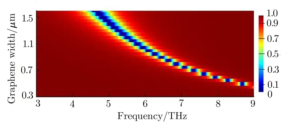
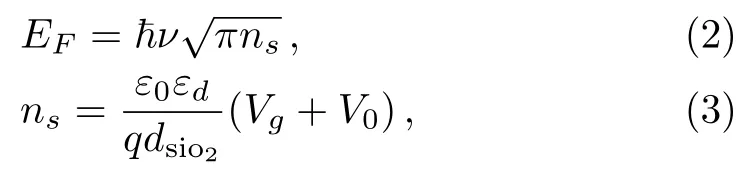
Fig.3 (Color online)Transmission spectra dependence on graphene ribbon width as a function of frequency with Fermi energy of 0.3 eV.
Transmission spectra of the device with graphene ribbon width of 1µm as a function of frequency and Fermi energy are shown in Fig.2(a).It is found that there exists a transmission dip in a broadband frequency range from 3 THz to 9 THz,which originates from the plasmon resonances in graphene ribbons.Moreover,the transmission dip is blue shifted as the Fermi energy increases,and this phenomenon can be explained by the surface plasmon resonance condition.The wave vector of surface plasmons along the graphene ribbons satisfies the conditions:kSSP∝ 1/W and kSSP=~ω2/(2α0EFc),[40]where W and α0represent the width of the graphene ribbon and the fine structure constant,respectively.Therefore,the resonant wavelength of graphene surface plasmons can be written asIt is obvious that the resonant wavelength is inversely proportional to the Fermi energy.Figure 2(b)shows the transmission spectrum of the structure for Fermi energy of EF1=EF2=0.3 eV and graphene ribbon width of 1µm,near-perfect absorption of incident THz wave around 6.02 THz is present,which paves the way of strong amplitude modulations.

Fig.4 (Color online)(a)Transmission spectra dependence on ribbon width as a function of frequency with different Fermi energies V1=0.27 eV and V2=0.33 eV.(b)Transmission spectrum at W=1 µm.(c)–(e)Field distributions((|EZ|)2)of graphene plasmon resonances in a unit cell of the graphene F-P microcavity(W=1µm)with the excitation frequency at 5.63(left dip),6.02(PIT peak),and 6.46 THz(right dip),respectively.In the investigations,the separation h is fixed at 3µm.
We can also know from resonant wavelength condition of the graphene surface plasmons that resonant wavelength is proportional to graphene ribbon width.Thus,resonant wavelength can also be adjusted by varying the graphene ribbon width,and the resulting transmission spectra dependence on graphene ribbon width as a function of frequency with Fermi energy of 0.3 eV are shown in Fig.3. The transmission dip is red shifted as the graphene ribbon width increases,and central frequency of the transmission dip can be adjusted from 4.5 THz to 9 THz.According to the results and discussion above,we can speculate that transmission dip will cover the entire THz frequency range if variation of graphene ribbon width and adjustment of graphene Fermi energy joint together,which provides a new method for strong amplitude modulations in the whole THz range.
When the metal gate voltages of two graphene ribbons are slightly different,a new transparency peak shown in Fig.4(a)emerges around the central of the original transmission dip,which is similar to the PIT effect in metallic plasmonic F-P systems.Figure 4(b)illustrates the transmission spectrum at W=1µm as a function of frequency with different Fermi energies EF1=0.27 eV and EF2=0.33 eV.It is found that transmission peak around 6.02 THz appears in the central of two transmission dips of 5.63 THz and 6.46 THz.The reason is attributed to the constructive interference between the reflected waves by two graphene ribbons.In order to verifying the underlin-ing physical mechanism,field distributions at frequency of 5.63 THz,6.02 THz,and 6.46 THz are illustrated in Fig.4(c)–4(e),respectively.It is obvious that when the excitation frequency is 5.63 THz or 6.46 THz,the local graphene plasmon resonances are excited in the up and down graphene ribbons,respectively,and almost all the THz waves are reflected.When the excitation frequency is 6.02 THz,up and down graphene ribbons are partially resonating,which constitutes a graphene F-P microcavity.Therefore,the excitation THz wave can pass through the graphene-based oscillator with high transmission.
Fig.5 (Color online)(a)Transmission spectrum for Fermi energy of EF1=EF2=0.3 eV and graphene ribbon width of 1µm.(b)Transmission spectrum for Fermi energy of EF1=0.27 eV and EF2=0.33 eV with graphene ribbon width of 1µm.(c)Modulation depth of this device as a function of frequency with graphene ribbon width varying from 0.3µm to 1.6µm.

Fig.6 (Color online)Transmission spectra with different thickness of SiO2insulator(a)–(d),quality factor of the device over a wide frequency range from 4 THz to 8.3 THz(e).
Traditionally,modulation depth(MD)is defined as MD=1−T/T0,where T is the minimum transmission,while T0is the maximum transmission.Furthermore,we also very concern about the tunable range of the modulator.Figure 5(a)shows the transmission spectrum for Fermi energy of EF1=EF2=0.3 eV and graphene ribbon width of 1µm.Figure 5(b)shows transmission spectrum with the same structure parameters as in Fig.5(a),but Fermi energy of the up and low graphene ribbons are 0.27 eV and 0.33 eV,respectively.Through comparison we can find that the MD of 6.02 THz reaches 95%,which means a strong amplitude modulation.Tunable range of the modulator with different graphene ribbon width is shown in Fig.5(c),and results demonstrate that MD in the frequency range from 4 THz to 8.3 THz is larger than 80%.
Up and down graphene layers in the structure are considered as two mirrors to constitute an F-P oscillator,the round-trip phase is controlled by the optical path difference between two mirrors.Therefore,the thickness of SiO2is important to the tunable properties of the THz modulator,and the transmission properties can be changed by adjusting the thickness of SiO2.Figures 6(a)–6(d)illustrate the transmission spectra at various values of d,it is found that the transmission spectra exhibit typical features of the F-P oscillations,such as,periodic,asymmetric,and blue-/red-shifted peaks with the variation of thickness of SiO2,which clarifies the F-P spectral features of the graphene based modulator.The Q factor can be used to measure resonant quality of devices,which can be defined as Q=fres/FWHM,where fresis the resonant frequency and FWHM is the full width at half maximum.Figure 6(e)shows the Q factor as a function of frequency with graphene ribbon width varying from 0.3µm to 1.6µm.It is obvious that as the resonant frequency increase,the Q factor decreases.
In order to tune the modulator conveniently,we further investigate tunable range of the modulator with graphene ribbon width fixed at 1µm.It is found that when the Fermi energy of the up-graphene ribbon changed from 0.07 eV to 0.47 eV(Fermi energy of the low-graphene ribbon is 0.06 eV higher than the up-graphene ribbon),the central frequency of the modulator changed from 4.2 THz to 9.4 THz with MD larger than 80%(Figs.7(a)–7(d)).The results reveal that we can simplify tuning the central frequency of the modulator in a wide frequency range through controlling the Fermi energy of the graphene ribbon.This tuning character is vital important and can be used as THz modulators and switches that cover the whole THz frequency range.

Fig.7 (Color online)(a)and(b)Transmission spectrum for Fermi energy of EF1=EF2=0.1 eV and EF1=EF2=0.5 eV,respectively.(c)Transmission spectrum for Fermi energy of EF1=0.07 eV and EF2=0.13 eV(d)Transmission spectrum for Fermi energy of EF1=0.47 eV and EF2=0.53 eV.In the investigations,graphene ribbon width is fixed at 1µm.
3 Conclusion
In summary,strong optical modulations based on periodically patterned graphene microcavity have been demonstrated.With electrically tunable Fermi energy,transmission properties of the graphene F-P microcavity are tunable in a wide frequency range.By optimizing the physical parameters,extremely strong optical modulations(larger than 95%)induced by the PIT effect is observed in a broadband THz frequency range.It is expectable that the MD can be further improved by optimizing the physical parameters.The potential for extremely large modulation depth and operation range covering the whole THz frequency promises the development of active high-performance spatial THz modulators in chip integrated photonic circuits.
猜你喜欢
杂志排行

Communications in Theoretical Physics的其它文章
- Impact of Colored Noise on Population Model with Allee Effect∗
- Entropy of Vaidya Black Hole on Event Horizon with Generalized Uncertainty Principle Revisited∗
- Anisotropy Effects and Observational Data on the Constraints of Evolution Dark Energy Models
- Multipolar Structure of Equilibrium Shear Flow Field in Toroidal Plasmas∗
- Improved Five-Parameter Exponential-Type Potential Energy Model for Diatomic Molecules∗
- Nontrivial Effect of Time-Varying Migration on the Three Species Prey-Predator System∗