基于数据线控制发光的A-IGZO薄膜晶体管集成AMOLED像素电路
2018-11-08王兰兰于天宝廖聪维黄生祥邓联文
王兰兰, 鲁 力, 于天宝, 廖聪维, 黄生祥, 邓联文
(中南大学 物理与电子学院, 湖南 长沙 410083)
1 Introduction
As promising alternative to the conventional thin film transistor liquid crystalline display (TFT-LCD), active matrix organic light-emitting display (AMOLED) owns many merits, such as high contrast ratio, short response time, wide viewing angle[1-5]. However, the mass production of AMOLED panel with large display dimension of high resolution is still difficult up to date, as performances of TFT array are far from satisfactory[6-8]. In recent years, Indium-gallium-zinc-oxide (IGZO) TFTs might be a favorable candidate for the commercialization of AMOLED in TV application[9-13]. This is because, compared with hydrogenated amorphous silicon (a-Si∶H) or polycrystalline silicon (poly-Si) TFTs, IGZO TFTs own the advantages of decent mobility, acceptable reliability and much improved uniformity over large area[14-15]. However, measurements show that there is still threshold voltage (VTH) shift of IGZO TFTs due to the voltage biasing of long operating time[16-17]. In additions, there is still non-uniformity ofVTHand mobility over the overall display panel. Thus, image quality of AMOLED panel might be reversely influenced[18]. Therefore, compensation scheme forVTHshift and non-uniformity ofVTHand mobility are still necessary[19 ].
The first in-array compensation AMOLED pixel circuit using IGZO TFTs was proposed by Chenetal.[20], where the current-scaling method was used to suppress mismatch current due to the threshold voltage shift and mobility variations. However, the current programming pixel circuits (CPPCs) are prone to have long settling time, especially in the case of OLED TV panel with ultra-high resolutions[21-22]. In later years, Moetal. proposed a voltage programming pixel circuit (VPPC) for the implementation of OLED TV[23], and threshold voltage can be compensated with the voltage bootstrapping method. Although the settling time is much decreased compared with CPPCs, the Mo’s method seems a little complicated as 5 TFTs and 2 capacitors are used, and 7 signals and power sources are required. Furthermore, the pixel current is still prone to shift due to mobility variations. And Kimetal. proposed another VPPC scheme by introducing a feedback structure to compensate mobility variations[24], assuming that the adjacent TFT to the driving transistor shares the same mobility. However, the previous pixel scheme requires much increased controlling signals, which increases the complex of external driving circuits and decreases the aperture ratio of pixels. Leeetal. pointed that the scan lines can be used to provide power source for the simplification of LTPS TFT pixels[25]. However, scan signal can’t be used as power source for the IGZO pixels and there is little investigation work on simplification of IGZO pixel structure up to date.
In the proposed method, a new VPPC is proposed for IGZO TFT AMOLED panel. Threshold voltage is extracted by the diode discharging method. And for pixel simplification, the data line is also used to control switching transistor (TS) between power supplier (VDD) and driving transistor (TD) for OLED.
2 Experiments
The proposed pixel circuit (a) and timing diagram (b) are shown in Fig.1. The illustrated pixel unit consists of three switching TFTs (T1, T2and TS), one driving transistor (TD) and one capacitor (CS). The OLED device is serially connected with the switching transistor TSand the driving transistor TD, which is used to provide gray level related current. Here T1and TSare used for the resetting ofVGduring the initialization phase, whereVGis the gate voltage of TD. The gate electrodes of T1and T2are connected to the sameVSCAN. Thus T1is also playing the discharging role for the programming ofVG. And the data voltage is transferred to the source electrode of TDthrough the switching transistor T2.
As shown in Fig.1(b), the voltage of scan line isVGHandVGLfor the selecting and the non-selection period, respectively. The voltage ofVDDisVDD_HandVDD_Lfor the emitting and non-emitting phases, respectively. And the voltage of data line isVREFandVHfor the initialization and emission phase, respectively. While for the programming phase,VDATAis with negative value. Fig.1(c) shows the array block diagram.
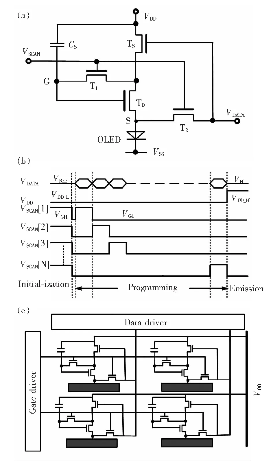
Fig.1 The proposed AMOLED driving method with pixel circuit(a), timing diagram(b) and block diagram(c).
Compared with the previous schematic, the main feature of the circuit is that the data line is connected with the gate electrode of TS. ThusVDATAis used to turn off TSto improve the accuracy of threshold voltage extraction for the programming phase, and also TScan be turned on withVDATAof high level. The operation details of the proposed pixel circuit are illustrated as follows.
2.1 Initialization Phase
For this phase,VSCANandVDATAare withVGHandVREFrespectively, andVDDisVDD_L. AsVREFis greater thanVDD_L, all the switching transistors,i.e. T1, T2and TSare turned on. As a result, G nodes of all the pixel circuits of AMOLED panel are pre-charged toVDD_L. On the other hand,VREFis less than the turn-on voltage of OLED. In consequence, OLED can be turned off to suppress the unexpected light emission for the initialization phase.
2.2 Programming Phase
In the programming phase, scan pulseVSCANare generated line by line, and data voltage can be transferred to the source electrode of TDthrough T2, thus OLED is also maintained off for contrast ratio improvement. Meanwhile, T1is also turned on and TSis switched off as the value ofVDATAis negative. Consequently, remaining charges of node G will be discharged through TDwhich is in a diode configuration. Thus by the end of programming phase, the gate voltage of TDequals the sum ofVDATAand threshold voltage of TD. TDworks in the saturation region due to the diode connection, and the transient response ofVGdischarging is
(1)
WhereμFE,CIare the field-effect mobility and gate capacitance per unit area, respectively.CGis the total capacitance in node G includingCSand capacitance existing adjacent TFTs .Also,WDandLDare the width and length of TDchannel.VDD_Lis the low level ofVDDandVDATAis the voltage of data line in the phase. By the integration of Eq.(1), transient ofVGis obtained:
VG=VDATA+VTH+
(2)
Wheret0andt1is the starting and ending time ofVGdischarging. The second and the third terms of Eq. (2) are combined monotone increasing function ofVTHand decreasing function of mobility. That is to say, for increasedVTHor decreased mobility, the discharging current will be decreased, thus largerVGcan be maintained. Therefore, there is a negative feedback loop for maintaining constant current for OLED pixels.
2.3 Emission Phase

(3)
whereCGPandCGIare the parasitic capacitance and intrinsic gate capacitance of TD, respectively. AsCGPandCGIare much smaller thanCS, Eq.(3) can be simplified as
(4)
consequently, the emitting current for OLED can be expressed as
(5)
whereVOLEDis the voltage of OLED’s anode in emission phase, and ΔVDDis the difference betweenVDD_HandVDD_L. As shown in Eq.(5), OLED current is a quadratic function ofVDATA, thus a wide programming range can be obtained by adjustingVDATA. And it is also proven thatVTHshift effect can be suppressed, asIOLEDis almost independent ofVTH. In additions, the pixel circuit can also compensate mobility variations as the third term in the bracket is reversely related with mobility.
Eq.(2) indicates that certain programming time (TP) is required forVTHextraction. IfTPis sufficiently long,VGis approximatelyVDATA+VTH. Thus thekfactor is introduced for evaluating the discharging result ofVG:
VG=(1-k)(VDATA+VTH),
(6)
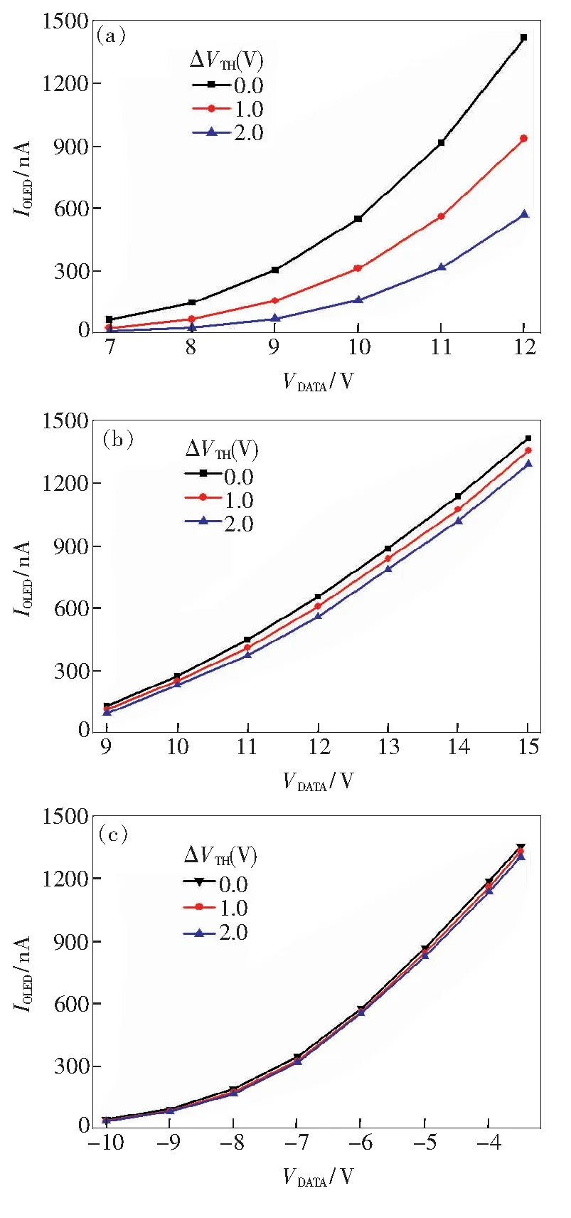
where 0 assuming that the mobility is 10 cm2/(V·s) andkis 0.1,TPis approximately 4 μs. Thus for the simultaneous emission driving scheme, the illumination time (TE) within the frame time (Tf) can be expressed asTE=Tf-TP×N, whereNis the number of rows of the panel. As a result, the effective illumination time will still be more than 12 ms, which is sufficient forHDformat. For evaluation of the proposed pixel circuit, simulations are carried out using SmartSpice. Tab. 1 shows the device parameters. The OLED device is modeled by a diode connected TFT and a capacitance in parallel.VDD_Lis 0 V for theVTHextraction period, andVDD_His 15 V for the light emitting period. The other signal voltages (i.e.VSCANVDATA) are listed in Tab.1. Fig.2 shows the transient response ofVGby simulation and calculation of Eq.(2). It is demonstrated that the calculatedVGmatches well with the simulation value. Thus the afore-mentioned derivations are reliable for pixel circuit design,i.e. choosing of TFT size, timing, and voltage. However, there are still voltage deviations in the light emitting period. This might be caused by capacitance variations of node G, which is voltage dependent instead of constantly maintained. Tab.1 Parameters of the proposed pixel circuit Fig.2 Transient waveform of VG by calculation and simulations with VDATA=-4 V Fig.3 demonstrates the transient response ofVGwith ΔVTHof 0, 1, and 2 V, for the programming time of 4 μs (a) and 20 μs (b), respectively. It is observed that,VGincreases linearly with that of ΔVTH. ThusIOLEDis independent ofVTHshift. AndVTHextraction is still of high accurate evenTPis decreased to 4 μs, which agrees with Eq.(8). However, ifTPis further decreased,VTHextraction can’t be completed, and the linearity of ΔVGwith ΔVTHwill be decreased, which introduce decaying ofIOLED. Fig.3 Transient waveform of IOLED with VTH shift of TD for programming time of 4 μs(a), and 20 μs(b). Fig.4 shows the comparison results ofIOLEDversusVDATAfor the 2T1C pixel circuit, and the conventional 4T1C structure[26],and the proposed one.IOLEDdecreases by more than 70% due toVTHshift of 2 V for the conventional circuit, which implies limited short lifetime. In the case of the conventional 4T1C scheme, decreasing ofIOLEDwithVTHshift can be effectively suppressed. However,IOLEDdiscrepancy is still larger than 15% byVTHshift of 2 V. This might be contributed to the variations of anode voltage of OLED withVTHshift. TheIOLEDdiscrepancy ofVTHshift can be decreased to be less than 5% in the proposed circuit. In additions, the tuning rang ofVDATAforIOLEDis comparable with the simple 2T1C structure, thus power consumption and complexity of external driving circuits are acceptable. Fig.4 Evolution of IOLED versus VDATA for VTH shift, with 2T1C pixel(a), and the conventional pixel circuit (b), and the proposed pixel circuit(c). Fig.5 Evolution of ΔIOLED error ratio versus VDATA for mobility variations with the 2T1C pixel circuit(a), and the conventional 4T1C pixel circuit(b), and the proposed pixel circuit(c). Fig.5 shows comparison of the current error by mobility variations for the 2T1C pixel circuit, and the conventional 4T1C circuit, and the proposed one. It is observed that, in the case of 2T1C circuit,IOLEDis increased by 12% and 7% with the mobility increasing of 30% and 15%, respectively. For the conventional 4T1C scheme and the proposed one, ΔIOLEDcan be suppressed to 9% and 7% with the mobility increasing of 30% and 15%, respectively. The improved mobility compensation efficiency matches well with afore the derivedIOLEDexpression as shown in Eq.(5). For the verification of circuit function, the proposed pixel circuit is implemented with discrete n-type MOSFETs[27-28]. And OLED is substituted by a resistor, scanning signals are provided by the FPGA platform using Verilog programming. As the anode voltage of OLED (VAnode) is in proportion toIOLED, thenIOLEDcan be derived by the measuredVAnodeusing oscilloscope. Fig.6 shows the transient response of the drain’s and gate’s voltage of TD. For the initialization phase, both the drain and gate electrodes of TDare initialized toVDD-L=2.3 V. And in the following programming phase, drain and gate electrode of TDare discharged to 1.7 V (=VTH+VDATA) through T2, with the data voltage(VDATA) of 0.8 V and with the threshold voltage(VTH) of 1 V. In the light-emitting phase, the voltage increase of the power supply (ΔVDD=0.8 V) is coupled to the gate of TDthroughCS, thus the measured voltage of the gate and drain electrodes of TDis 2.5 V and 3.3 V respectively. Fig.7 shows the measuredIOLEDwith the supplied n data voltageVDATA. The measuredIOLEDis approximately a quadratic function ofVDATAin the caseVDATAis less than 1.25 V. However, the measuredIOLEDstarts to saturate withVDATAexceeding 1.25 V. And this is attributed to the driving limitation of FPGA board. To sum up, the programming ability of the proposed pixel circuit is well proved. Fig.6 Transient response of TD with the drain voltage(a), and the gate voltage(b). Fig.7 Relationship between VDATA and IOLED of 4T1C pixel circuit In this paper, a new IGZO TFT pixel circuit with simplified structure for AMOLED panel with high resolutionis was proposed. It features using the data line to switch the controlling transistor betweenVDDand the driving transistor. Thus only scanning signals, data signal andVDDsupply line are used for a single pixel circuit, and the scanning driver can be as simple as the conventional 2T1C display. Performance comparisons are carried out between the proposed circuit, the 2T1C pixel, and the conventional 4T1C scheme. Compensating efficiency of the proposed circuit is improved concerning threshold voltage shift and mobility variations.IOLEDdiscrepancy is decreased to be less than 5% and 9%, withVTHshift of 2 V and mobility increasing of 30%, respectively. And it also features much decreased transient current during programming phase. Measurements using discrete FETs are carried out to verify the driving ability of the proposed 4T1C pixel circuit. The measuredIOLEDversusVDATAmatches well with the analysis. The disclosed results verify the proposed scheme is suitable for realizing AMOLED panel with high resolution.3 Results and Discussion


4 Conclusion