用于智能锁的超低功耗系统的设计与应用
2018-10-09王炼红陈颖
王炼红 陈颖
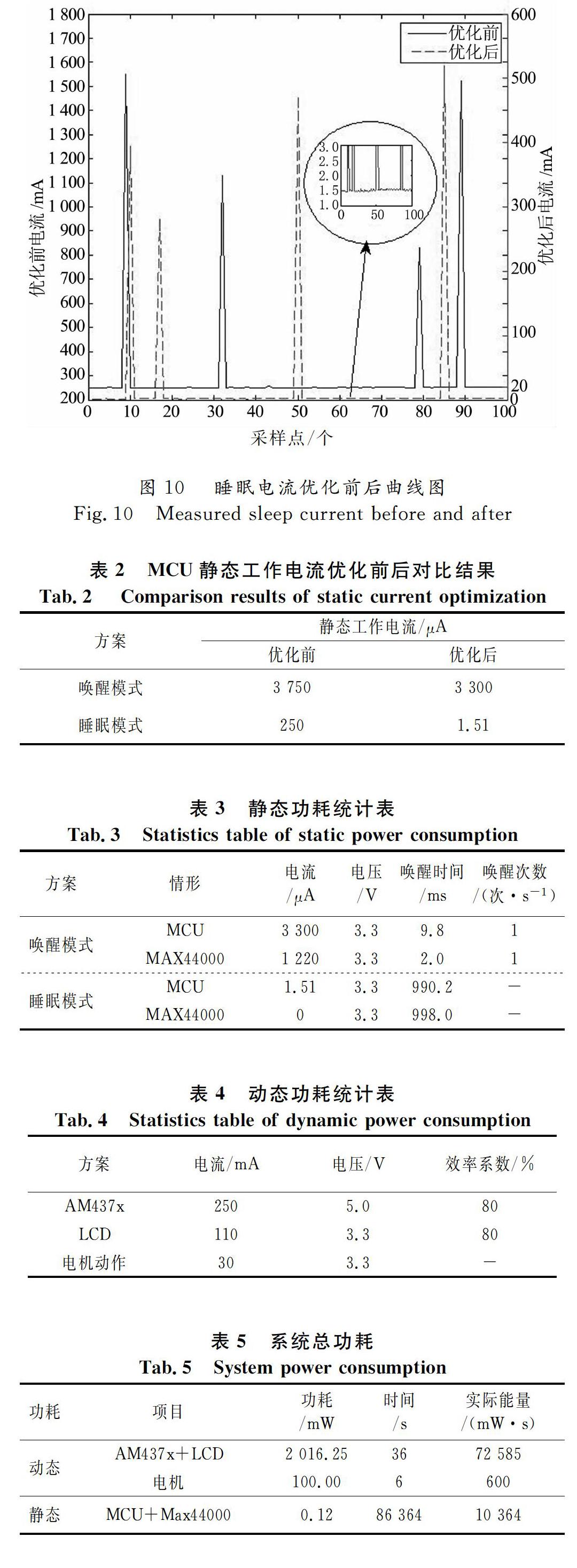

摘 要:为解决现今指纹锁的高性能和低功耗之间的矛盾,提出了一种基于双核架构的嵌入式系统,采用TI公司AM437x高性能处理器移植识别算法;具有超低功耗的AVR单片机MEGA8微控制器作为主控芯片,以控制非接触启动、红外灯、电机驱动等外围设备,保证系统具有较低的待机功耗.通过设置主控芯片的超低功耗睡眠模式,使得系统大部分时间处于低功耗状态,利用非接触式启动模块控制高耗能识别模块仅在需要的时候上电启动,从而大大降低系统的功耗.综合测试表明,系统休眠时MCU静态工作电流低至1.51 μA,唤醒时电流优化至3.3 mA,8节干电池使用寿命为638 d.相比现有设计方法,兼具更低的功耗和更高的性能.
关键词:超低功耗;静态电流;电源管理;智能锁
中图分类号:TP368.2 文献标志码:A
Abstract:This paper presented an embedded system based on dualcore architecture to solve the contradiction between high performance and low power consumption of today fingerprint lock. TI's AM437x highperformance processor was used to transplant identification algorithm, with AVR microcontroller MEGA8 microcontroller of ultralow power as a master chip to control noncontact start, infrared light, motor drive and other peripherals to ensure that the system has a lower standby power consumption. By setting the ultralow power sleep mode of the master chip, the system is in a low power state for most of the time, and the noncontact startup module controls the high power consumption identification module to power up only when it is needed, thus greatly reducing the power consumption. Comprehensive test shows that the static operating current is as low as 1.51 μA when the system is in sleep mode, while the wakeup current is optimized to 3.3 mA. The maximum system life of six dry cells is 638 days. Compared with the existing design methods, the system has both lower power consumption and higher performance.
Key words:ultralow power consumption;static current;power management;intelligent lock
近年来,随着生物识别技术和电脑科技的迅速发展,指纹识别技术已广泛地进入大众的视野.随着指纹技术和半导体技术的发展,指纹锁已被广泛应用到军事、保密机构等[1-3].
目前指纹识别系统主要采用具有高速数据运算能力的DSP或者基于ARM核的处理器芯片或者高性能现场可编程门阵列FPGA来完成算法处理和识别.Wu等人[4]应用基于ARM内核的STM32F103ZE微处理器完成指纹处理以及外设模块的控制,待机功耗为0.21 μA,但识别速度不高.Mondol等人[5]使用高性能FPGA芯片集成优化后的算法,获得了更高的识别率,但功耗比较高.杨伟钧[6]采用TI公司的TMS320C5509A作为处理器,实现指纹算法的移植,系统能稳定运……