A Pathway to Explore the Hidden Specialty in the Design of Fifteen Level Inverter in Grid Connected PV System
2018-07-12GopinathandRajvikram
C. Gopinath and M. Rajvikram
Abstract: This research paper proposes a single phase fifteen level inverter for a grid connected PV system. The proposed inverter is also called cascaded asymmetric multilevel inverter. By adopting appropriate hybrid modulation technique improved output voltage is obtained with minimum number of power electronic switches. By reducing the number of gate triggering circuits of the switches, the size and power consumption of the driving circuits can be reduced. The total harmonic distortion of the output of the inverter is improved by this inverter. The proposed inverter developed by cascading a full bridge inverter with modified H bridge multilevel inverter. The validity of the proposed system is verified through MATLAB simulations.
Keywords: Hybrid modulation, multilevel inverter, photo voltaic system, grid connected inverter.
1Department of Electrical and Electronics Engineering, Sri Venkateswara College of Engineering(Autonomous), Sriperumbudur, Tamilnadu, India.
*ACorresponding Author: C. Gopinath. Email: cgopinath@svce.ac.in; drcgopinath@gmail.com.
1 Introduction
In current scenario, there is thirst for advanced inverter designs which lead the design of multi level inverters, More commonly single-phase five-level inverter are controlled by two novel Pulse Width PWM techniques are designed based on minimum switching power loss and minimum Total Harmonic Distortion (THD). In a single-phase five-level inverter employing six switches, in all the PWM proposed techniques. It requires four switches operate at switching frequency and the other two switches in turn operate at line frequency, whereas there are also some PWM proposed technique which requires only two switches operate at switching frequency and the others operate at line frequency[Sonti, Jain and Bhattacharya (2017)]. Broad applications of dc-dc converters are conceptually explained in many surveys and summarized with comparative study of different voltage-boosting techniques. DC-DC converters with voltage boost capability are widely used in a large number of power conversions. The permutations and combinations of the various voltage-boosting techniques with additional components in a circuit allow for numerous new topologies and configurations, which are often confusing and difficult to follow. Therefore, to present a clear picture on the general law and framework of the development of next-generation step-up DC-DC converters, this paper aims to comprehensively review for classifying various step-up dc-dc converters based on their characteristics and voltage-boosting techniques. In addition, the advantages and disadvantages of these voltage-boosting techniques and associated converters are discussed in detail. Finally, broad applications of dc-dc converters are presented and summarized with comparative study of different voltage-boosting techniques [Sonti and Jain (2017)]. A power conditioning system (PCS) using multiple module-integrated converters and a single sourced 27-level asymmetric cascaded H-bridge multilevel inverter without regeneration for photovoltaic applications. There is a scheme called PCS with the control scheme which is implemented similar to the work that we have included in this research work. It gives a perfect floor to establish effective results [Kadam and Shukla (2017)]. The common mode (CM) leakage current needs to be addressed carefully in order ensure the smooth operation of transformerless grid connected PV system, In present scenario the conceptual implementation of novel multilevel transformerless inverter topology which completely eliminates CM leakage current by connecting grid neutral point directly to the PV negative terminal, thereby bypassing the PV stray capacitance. It provides a low-cost solution consisting of only four power switches, two capacitors, and a single filter inductor [Liu, Abu-Rub, Ge et al. (2016)].
Pulse width modulation (PWM) technique is purely meant for the minimization of the leakage current in the grid-connected/stand-alone transformerless photovoltaic (PV)-cascaded multilevel inverter (CMLI).PWM technique is integrated with the MPPT algorithm and is applied to the five-level CMLI. Furthermore, using the proposed PWM technique the high-frequency voltage transitions in the terminal and common mode voltages are minimized [Chattopadhyay and Chakraborthy (2017)]. Among the various kinds of renewable energy sources solar and wind energy become very attractive due to the abundant nature and advancement in power electronic equipments. Photovoltaic sources are employed in many solar based applications to extract the electrical energy from the sun as they have an advantage of being reliable and pollution free. Also it is maintenance free. Photovoltaic (PV) sources are employed in many solar based applications to extract the electrical energy from the sun as they have an advantage of being reliable and pollution free, also it is maintenance free. PV inverter is the main part of the PV system used to convert the dc voltage from the PV panel into AC Voltage to be fed into the grid. Enhancing the output waveform diminishes its corresponding harmonic content also size of the filter. There are numerous inverter topologies are available for grid connected PV system [Sonti and Jain (2017)]. The main problem focused in the paper is total harmonic distortion and to improve the output voltage. If a power electronic switch used in a high voltage inverter, then it cannot be operate at high switching frequency. Hence their switching frequency is restricted. Hence the operating voltage of the device must be reduced to use high speed switches. High speed switches contributes very low harmonic content compared to low speed switches. Multilevel inverters can reduce device voltage and output harmonics by increasing number of output voltage levels. In single-phase multilevel inverters, the most widely used techniques are diode clamped inverters, flywheel capacitor inverters and cascaded H-bridge inverter (CHB).Among all this inverter cascade H bridge inverter drawn more attention due to its simplicity and circuit modularity. Varity of modulation techniques can be implemented only in CHB.
2 Proposed method
The Block diagram of the proposed inverter is shown in Fig. 1. This proposed single phase inverter is combination of a modified H-bridge inverter (seven level inverter) and conventional H bridge inverter connected in parallel. The upper H bridge inverter is conventional, whereas the lower H bridge is a modified H bridge inverter developed in[Rahim, Chaniago and Selvaraj (2011)]. The intention of using the modified H-bridge configuration is to reduce the switching devices, power diodes, capacitors and isolated DC source. Upper and lower inverters are connected with individual PV arrays. Since the proposed inverter is an asymmetrical inverter voltage of the lower inverter is higher than the upper inverter. Voltage from the PV array is boost up by the dc-dc converter to the level required by grid. Current injected into the grid is filtered by Lf.

Figure 1: Block diagram of the proposed inverter
2.1 Hybrid modulation
Hybrid modulation technique reduces the switching losses of the proposed inverter by appropriate switching pattern. Proposed inverter is asymmetric inverter hence the input voltages of upper and lower inverter are not the same. Since power fed from the lower inverter is more than the upper inverter, it is switched at low frequency and the upper inverter is switched at high frequency.
2.2 Lower inverter
Three reference signals (Vref1Vref2Vref3) were compared with the carrier signal (Vcarrier).The reference signals has the equal magnitude and frequency and was in phase with each other by an offset value. But they were shifted consequently in y axis by a constant value.Vref1was compared with Vcarrieruntil its amplitude is higher. Vcarriercompared with Vref2till its amplitude is higher. Vref3compared with Vcarrieruntil it reaches zero. Once Vref3had reached zero, Vref2would be compared until it reaches zero. Then Vref1would be compared with Vcarrier. Fig. 4 shows the resulting switching pattern. Switches S1, S3, S5and S6switched at a frequency of carrier signal were as S2and S4switched at fundamental frequency. Lower inverter produces seven level output voltage. Lower inverter supplies more voltage (240 V) to the grid and switched at low frequency.
2.3 Reference wave and carrier wave generation
The simulation results were carried out by using MATLAB/SIMULINK environment to prove that the proposed inverter can be implemented practically. It helps to observe the switching strategy of fifteen level inverter. Switching pattern for the lower inverter is generated by comparing three reference signals and triangular carrier signal shown in Fig.1. The resulting PWM signals are shown in the Fig. 2. The modulation index determines the shape of the inverter output voltage. The lower inverter is switched at low frequency(50 Hz) and the upper inverter has high frequency (10 kHz). Upper inverter dc input voltage is 65 volts and lower inverter dc bus voltage is six times of upper inverter that is 390 volts. The switching signals are developed by the equations as described. Finally the desired waveform of seven level stepped waveform is obtained at lower level inverter which is shown in Fig. 3.
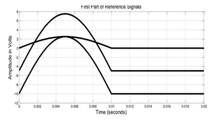
Figure 2: First part of reference signals

Figure 3: Second part of reference signals

Figure 4: PWM signal generation of lower inverter
2.4 Arithmetic equation for reference signal and pulses generation
Reference wave form of the lower inverter is generated by the following equations,The overall reference signal, Vref= sin ɷt
Three reference signals,
Vref1= |Vref|*12.5
Q3= (K1+K3)|| C
Vref3= |Vref|*12
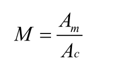
These reference signals are further divided into two parts.Vref1= {Vref11if 0 Vref12if T/2 Vref2= {Vref21if 0 Vref22if T/2 Vref3= {Vref31if 0 The real life and spirit of this magical elf lives forever in your heart, my heart, Mom’s heart and in the hearts and minds of all people who believe in the joy that giving to others brings Vref32if T/2 T = Time period Q5= Q1’+ (K2+K3+K4)||C K6= {1 if Vref32>0 0 if Vref32<0 Q1=(K3+ K5)|| C Switching signals Don t behave like the cow that kicks the pail over after it has filled it with milk, but continue your journey with me, and when we get to the capital you can sell me to the King as a servant girl C= Carrier wave “||” represents comparison“+ “denotes logical OR operation But when she went up to the Prince s room he was again asleep, and, let her call him, or shake him, or weep as she would, he still slept on, and she could not put any life in him Q2= (1 for 0.01 Vref2= |Vref|*2 It was a luxury the ragtag team obviously could not afford. Well, we ended up walloping them. We took every weight class. And as each of their boys got up from the mat, he swaggered around in his tatters with false bravado8, a kind of street pride that couldn t acknowledge defeat. Q4= (1 for 0 PWM switching signals generation The Prince without paying any further heed68 to him or to his whistling returned to the pretty gazelle, saying: Well! are you satisfied now? Since you can talk, pray tell me instantly what all this is about, and how you happen to know my name Q6= Q3’+ (K1+K2+K3)||C Q’= compliment of Q • Switching pulses for switch Q6: First part of the Q6is obtained by comparing Vref1and Vref2with the carrier signal as shown in the Fig. 2 and the second part is obtained by Vref2and Vref3with the carrier signal and second part of Vref3compared with the carrier until Vref3lesser than carrier amplitude. Each reference signal is identical with each other and displaced by an offset value -5.These three signals are generated and compared with the carrier wave (triangular wave)of frequency 10 KHz. Frequency of the reference signal is 50 Hz. In order to reduce the switching losses of the proposed inverter hybrid modulation scheme is used. Switching pulses are generated by comparing three reference signals Vref1,Vref2, and Vref3and a carrier signal Vcarrier. Fig. 2 shows the switching pulse generation of seven level inverter. All three reference signal had same frequency and amplitude with an offset value equivalent to the amplitude of carrier signal. The reference signals were compared with the carrier signal simultaneously. Frequency of the reference signal is 50Hz and the carrier signal is 1 KHz. Triangular wave is a carrier signal of frequency 1 KHz and amplitude one and modified sine wave is modulation signal of frequency 50 Hz (fundamental frequency) with the amplitude of 2.5 each waves are displaced by a constant value as shown in Fig. 4. • Switching pulses for switch Q1: First part of the reference signal Vref3is compared with the carrier signal until Vcarrieris greater than Vref3and Vref1is compared with the Vcarrieruntil Vref1is greater than Vcarrier. • Switching pulses for switch Q2: It is an ordinary gate pulse of fundamental frequency with first half of the period turned OFF and second of the period turned ON. But before he had gone far his friend the wolf stood before him and said, Dear Prince, why are you so cast down? It is true you didn t succeed in catching16 the bird; but don t let that discourage you, for this time you will be all the more careful, and will doubtless catch the horse • Switching pulses for switch Q3: Reference signal Vref1is compared with the carrier signal until it exceeds the peak amplitude of the carrier signal Vcarrierand second part of the Vref3is compared with Vcarrieruntil carrier wave amplitude is greater than the reference signal. • Switching pulses for switch Q4: It is an ordinary gate pulse of fundamental frequency with first half of the period turned ON and second of the period turned OFF. As these two children would possibly inherit the kingdom, it was natural that their people should take a great interest in them, and it fell out that all the tranquil10 and peace-loving citizens desired that Placida should one day be their Queen, while the rash and quarrelsome hoped great things for Vivien • Switching pulses for switch Q5: First part of Vref2reference signal is compared with Vcarrieruntil less than Vref2for a first carrier frequency and both are compared until Vcarriergreater than Vref2and (inverted signal of first part of Q5) first part of reference signal Vref3is compared with the carrier signal until Vcarrieris lesser than Vref3and Vref1is compared with the Vcarrieruntil Vref1is lesser than Vcarrier. The second part of Q5is obtained by comparing Vref1and Vref2with the carrier signal as shown in Fig. 2. Every year at Christmas, his ex-girlfriend would return from Vancouver to look him up. He was aware that she still held some hope of rekindling2() the past romance with him. He did not wish to mislead her in any way. So he would always get one of his girl friends to pose as his steady whenever she came back. Q1, Q2, Q3, Q4, Q5and Q6are the switching signals of lower inverter. Table 1: The inverter output voltage for various time duration Limit of duty cycles is 0.23-0.33. The duty cycle is not fixed due to the tracking process of the maximum power point voltage. In the above expression the worst condition is the minimum input voltage condition, thus maximum and minimum duty cycle is taken into consideration for further designing. Theoretically modulation index can be defined as the ration of amplitudes of modulating signal to the carrier signal. 19. But not one of them could slip the ring over the tip of her finger: The ring is very much like Cinderella s slipper in that it only fits its owner. In some versions of the story, hopeful girls cut off their fingers hoping to get the ring to fit. The exclusivity of the fit also implies the divine and regal heritage of the owner.Return to place in story. Since the proposed inverter uses three carrier signals, the modulation index is, Where Acis the peak-to-peak value of the carrier signal and Amis the peak value of the voltage reference signal Vref. Level of the output voltage can be varied by varying the modulation index. Reference wave form of an upper inverter is combination of saw tooth and positive half cycle of sine wave. Fig. 5 shows the reference wave form of upper inverter. Figure 5: Upper inverter-reference waveform The above reference wave is compared with the carrier wave to generate PWM pulses for power switches in upper inverter. The above reference wave is compared with the carrier wave to generate PWM pulses for power switches in upper inverter. Upper inverter produces three level output voltage. Carrier wave of the upper PWM is triangular wave form of 1 KHz with unity magnitude. Upper inverter supplies less voltage to the grid and switched at high switching frequency. The schematic diagram of grid connected PV system is shown in the Fig. 6. Cascaded upper and lower inverter generates fifteen level output voltage. Output Voltages of both inverters summed up and gives the resultant voltage. Proposed inverter is of asymmetrical type; hence voltage across the capacitor in lower H-bridge is two time the magnitude of upper bridge capacitor. (i.e. Vdc2= Vdc3= Vdc3= 2Vdc1). Figure 6: Schematic diagram of grid connected PV system Hence DC-link voltage of lower H-bridge is six times that of upper H-bridge. (i.e. Vdc,low=6Vdc1). If we take PV panels of equal rating upper H-bridge inverter needs single PV panel as input, whereas lower H-bridge inverter needs six PV panels. Thus most of the power fed to the load is from lower level inverter. Lower H-bridge inverter is of generating seven level output (6Vdc1, 4Vdc1, 2Vdc1, 0, -2Vdc1, -4Vdc1, -6Vdc1). Upper conventional inverter generates three level output (Vdc, 0, -Vdc). Boost converter boost up the voltage to the inverter output matches voltage the grid voltage. Input of the boost converter is output of the PV panel. According to the duty cycle which is being calculated by the MPPT algorithm the boost converter output also varies to track the maximum power from the PV panel. There are two boost converters are used in proposed system, there are upper boost converter and lower boost converter. Fig. 7 shows the simulink model of fifteen level inverter. Here both the upper and lower inverters are cascaded together and forms an asymmetrical fifteen level inverter. Three level output voltage of upper inverter and seven level output voltage of lower inverter are cumulatively added and produce fifteen level output voltage. Figure 7: Simulink model of fifteen level inverter Figure 8: Switching signals of lower inverter The Fig. 8 shows the switching signals of the switches, where the switching frequency of Q1, Q3, Q5and Q6pulses propositional to the carrier frequency but the switching frequency of the pulses Q2and Q4are equal to the fundamental frequency 50 Hz. Figure 9: Switching signal of upper inverter Switching pulses of upper Inverter is shown in Fig. 9 whose frequency is 5 Khz. Output voltage of upper and lower Inverter is shown in Fig. 10 and Fig. 11 respectively. Figure 10: Upper inverter output voltage Figure 11: Lower inverter output voltage Figure 12: Fifteen level inverter output voltage Output Voltage of Cascaded Inverter (upper and lower) of frequency 50 Hz shown in Fig. 12. Fig. 13 shows the simulink model of grid connected inverter fed PV system. Input to the inverter is taken from the PV panel. Output power from the PV panel is not constant because of the change in solar irradiance. MPPT algorithm is implemented to optimize the input power to the inverter from the PV panel and maintain the output voltage constant even though the solar irradiance changes with respect to time. Figure 13: Simulink model of grid connected fifteen level inverter for PV system Figure 14: Simulink model of Perturb and Observe MPPT algorithm Fig. 14 shows the simulink model of Perturb and Observe MPPT algorithm. The above simulink model is formed as per P&O algorithm. Saturation value is set between 0.33 to 0.23 by duty cycle calculation (Appendix). Figure 15: Grid voltage Inverter output voltage is approximately matches with the grid voltage as shown in Fig. 15. Analysis of total harmonic distortion (THD) The THD analysis of three level inverter is shown in the Fig. 16 whose value is 31.70%. Figure 16: THD analysis of three level inverter The THD seven level inverter is shown in the Fig. 17 whose value is 11.90%. With the first sunbeam she broke into the room, but there she found no prince and no princess--nothing but the two pieces of firewood, which lay in the bed, and stared, and spoke20 not a word Figure 17: THD analysis of seven level inverter The THD analysis of grid connected fifteen level inverter is shown in the Fig. 18 whose value is 4.99%. Figure 18: THD analysis of grid connected fifteen level inverter It is observed that the THD value of grid connected fifteen level inverter for PV system is less than 5% which is clearly depicted in Tab. 2. Table 2: Comparison of different multilevel inverters with respect to the THD This paper has proposed a novel single phase fifteen level grid connected inverter for PV systems. The PV uses P&O MPPT algorithm for maximizing the energy to the inverter.Hybrid modulation scheme is adopted to reduce the switching losses of the proposed inverter. The simulations are carried out in MATLAB/Simulink environment. The proposed inverter has upper and lower inverter. The upper inverter produces three level output voltage and lower inverter produces seven level output voltages. By cascading both these inverters produces fifteen level inverter. The proposed inverter has improved the output voltage of the inverter. The total harmonic distortion is also reduced to less than 5%.


2.5 Upper inverter

2.6 Grid connected PV system

2.7 Boost converter
3 Results and discussion


3.1 Simulink model of fifteen level grid connected inverter for PV system

3.2 Simulink model of Perturb and Observe (P&O) MPPT algorithm


4 Conclusions
杂志排行

Computer Modeling In Engineering&Sciences的其它文章
- Modeling the Spike Response for Adaptive Fuzzy Spiking Neurons with Application to a Fuzzy XOR
- Extrapolation M ethod for Cauchy P rincipal V alue I ntegral with C lassical R ectangle R ule on I nterval
- Modeling and Analysis of Global and Diffuse Solar Irradiation Components Using the Satellite Estimation Method of HELIOSAT
- Numerical Investigation of the Effect of Sorption Time on Coal Permeability and Gas Pressure
- Theory and Calculation of the J-Integral for Coupled Chemo-Mechanical Fracture Mechanics