基于USB 3.0接口的高速数据传输系统设计
2017-03-23宋中喆裴东兴杨少博
宋中喆+裴东兴+杨少博
摘 要: 针对目前存储测试系统中存有的数据传输慢,经常出现错误的显著问题,设计基于USB 3.0接口的高速数据传输系统。该设计以FPGA作为主控芯片,采用负延迟与乒乓缓存的方式将A/D转换的数据高速缓存到DDR2 SDRAM中。设计了GPIF Ⅱ 通用可编程接口和手动 DMA 通道,实现了USB 3.0同步从FIFO模式的高速数据传输。系统分析测试和实验结果表明,该系统实现了数据的高速可靠传输,能有效解决大容量数据采集后的数据高速传输问题。
关键词: 存储测试; USB 3.0接口; 高速数据传输; 负延迟; 乒乓缓存
中图分类号: TN919.6?34; TP334.7 文献标识码: A 文章编号: 1004?373X(2017)04?0159?04
Design of high?speed data transmission system based on USB 3.0 interface
SONG Zhongzhe1,2, PEI Dongxing1,2, YANG Shaobo1,2
(1. National Key Laboratory for Electronic Measurement Technology, North University of China, Taiyuan 030051, China;
2. MOE Key Laboratory of Instrumentation Science and Dynamic Measurement, North University of China, Taiyuan 030051, China)
Abstract: Since the current memory test system has the prominent problems of low data transmission speed and frequent fault occurrence, a high?speed data transmission system based on USB 3.0 interface was designed. The FPGA is taken as the main control chip of the design. The modes of negative delay and Ping?Pong cache are adopted to cache the data transformed through A/D into the DDR2 SDRAM with high speed. The general programming interface GPIF II and manual DMA channel were designed to realize the high?speed data transmission based on USB 3.0 synchronous slave FIFO mode. The system analysis, test and experimental results show that the system has realized the high?speed and reliable data transmission, and can effectively solve the high?speed data transmission problem occurring after large?capacity data acquisition.
Keywords: memory testing; USB 3.0 interface; high?speed data transmission; negative delay; Ping?Pong cache
0 引 言
随着当前存储测试系统[1]中存储容量的急剧增加,对数据的传输速度的要求随之也越来越高,此外在某些需要对数据进行实时传输处理的场合,人们对数据传输系统的速度要求也越来越严格[2]。本实验室以前一直在使用USB 2.0接口作为存储测试系统的数据传输接口,但受限于其理论最大480 Mb/s的传输速度,现在已逐渐难以满足数据传输的要求。新一代的 USB 3.0继承了 USB 2.0 的所有优势,能够向下兼容 USB 2.0,且在USB 2.0的基础上新增了超速传输模式,理论传输速度[3?4]可高达 5 Gb/s。并且在固件程序开发、电源管理等方面有了更好的提高。故而USB 3.0接口可以很好地解决那些问题。在未来的几年内,USB 3.0 必定能够较好地应对数字时代要求的高速性能和可靠互联性[5]。
1 系统总体方案设计
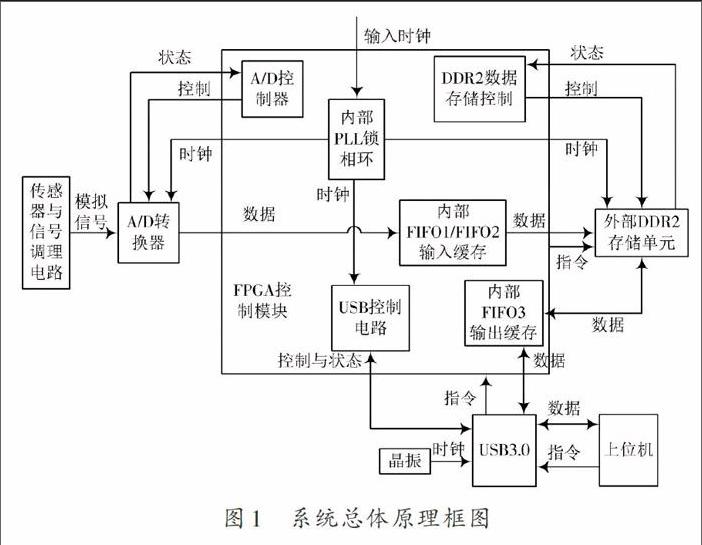
本文设计的系统主要包含五部分:传感器与信号调理电路、ADC数据转换电路、DDR2数据存储单元、FPGA控制电路和USB 3.0数据传输接口。……