氧化铟锡(ITO)自组装修饰及其对有机电致发光器件性能的影响
2015-12-01邓瑞平周亮李磊姣张洪杰
邓瑞平 周亮李磊姣 张洪杰
(中国科学院长春应用化学研究所稀土资源利用国家重点实验室,长春130022)
氧化铟锡(ITO)自组装修饰及其对有机电致发光器件性能的影响
邓瑞平周亮*李磊姣张洪杰*
(中国科学院长春应用化学研究所稀土资源利用国家重点实验室,长春130022)
设计合成了一种新型的有机硅氧烷Cz-Si,并将其用于ITO自组装修饰。制备的Cz-Si具有较好的稳定性,可以在空气中对ITO进行自组装修饰,实验操作简单。为考察ITO自组装修饰对有机电致发光器件性能的影响,分别以修饰后的ITO(ITO/ SAM)及不修饰的ITO(unmodified)作阳极,制备了一系列有机电致发光器件ITO/SAM(or unmodified)/NPB(40~50 nm)/Alq3(60 nm)/ LiF(1.0 nm)/Al。实验结果表明,ITO自组装修饰后器件性能可以得到显著提升,研究认为这与其调控ITO/有机层界面的电子能级、粗糙度以及界面一致性有关。
ITO修饰;自组装;有机电致发光器件
0 Introduction
Interfaces play a pivotal role for the performance of the organic light-emitting diodes(OLEDs).Anode/ hole transportation layer(HTL)is one of the most importantinterfaces,whichdeterminesthehole injection efficiency.Indium tin oxide(ITO)has been the most commonly used anode in OLEDs due to its high conductivity and transparency.Tailoring of ITO surfacepropertiesrepresentsahighlydesirablemethod to improve the device performance.There are many physical and chemical treatments to improve the ITO/HTL interface characteristics,aiming at modulating the work function of the electrode,tuning the balance of carrier injection,smoothening the surface roughness,and eliminating the disparity of ITO/HTL interface,such as O2plasma[1],UV ozone[2],chlorination[3],or coating the ITO with a buffer layer,such as copper phthalocyanine(CuPc)[4-5],poly 3,4-ethylene dioxythiophene:polystyrene sulfonate:(PEDOT:PSS)[6-7], CHFx[8-9],etc..Insertion of transition metal oxide thin film between the ITO and the organic layer has also been another efficient way to improve the carrier injection,such as MnO[10],MoO3[11],Al2O3[12],and WO3[13].
Although there are numerous ways to improve the surface properties of ITO,one of the most successful modifications is the use of monolayers based on organic molecules with widely variable and functional groups.Introducing a self-assembled monolayer(SAM) on ITO surface allows the molecular engineering of the ITO/organic interface,and results in the fine control of the interfacial chemistries and electronics. In particular,both surface energy matching and work function compatibility at ITO/HTL interface can be remarkably improved.For the formation of robust monolayers on ITO,a variety of different functional groups can be used,such as phosphonic acids[14], carboxylic acids[15],thiols,alcohols,and organosilanes (e.g.,alkoxy-and chlorosilanes)[16-17].Organosilanes have found great utility in the modification of metal oxides in general[18-19].Many groups have shown their brilliant work on this field.Huang Q.et al[20-21]achieved remarkable enhancement of the device performances by ITO SAM modification,but the organosilane(e.g., chlorosilanes)they used were highly sensitive to moisture[16-21],and the modification experiments should be operated under rigorous protection,which makes experimental operation complex.
In this work,a novel alkoxysilane Cz-Si was synthesized and used as an active reagent for SAM modification on ITO surface.The synthesized Cz-Si is stable in air,and the SAM modification operation could be processed without any protection.A series of devices were fabricated with ITO/SAM as anodes,and the effect of SAM on the device performance was investigated.Thedeviceperformancecouldbe improvedsignificantlybyITOCz-Si-SAMmodification.
1 Experimental
1.1Materials and instruments
9-ethyl-9H-carbazol-3-amine(95%)and triethoxy (3-isocyanatopropyl)silane(95%)were purchased from Sigma-Aldrich.NPB and Alq3(99.99%)were purchased from Beijing Yilaite Optoelectronic Materials Company.
1H NMR spectra were recorded on a Mercury Plus-400 spectrometer in DCCl3.Cyclic Voltammetry curve of Cz-Si was measured by CHI600B analyzer (Shanghai Chenhua Instruments Company).XPS data were taken by Thermo ESCALAB 250.
1.2Synthesis of Cz-Si
1.05g 9-ethyl-9H-carbazol-3-amine(5.0 mmol) was added into a 100 mL three-necked flask,and dissolved by 30 mL anhydrous chloroform.The solution of 1.33 mL(5.0 mmol)triethoxy(3-isocyanatopropyl) silane in 10 mL anhydrous chloroform was dropped into the reaction flask slowly under stirring.The reaction mixture was refluxed for 12 h,and then most oftheexcesssolventwasevaporated,andthe remainder was cooled to room temperature.After that the rest reaction solution was poured into 300 mL petroleumether,andalargeamountofwhite precipitate appeared.After filtration,the precipitate was washed with petroleum ether several times,and dried in vacuum.The product(named as Cz-Si)was 1.93 g(yield 84%).The purification of the crude product:the product was dissolved in a little of chloroform again,and a large amount of petroleum ether was added,and then the precipitate was washed and dried.1H NMR(CDCl3,400 MHz):δ 0.61(t,2H), 1.15(t,9H),1.22(q,5H),3.24(broad,2H),3.73(m, 8H),7.2~7.5(m,7H),7.98(broad,1H),8.07(1H).
1.3Characterization of the electrochemical property of Cz-Si
Cz-Si was dissolved in CHCl3(1.0 mmol·L-1).n-Bu4N+(ClO4)-solution(0.1 mol·L-1in CHCl3)was used as the supporting electrolyte.Cyclic voltammetry(CV)characterization was carried out on a CHI 600B electrochemical workstation with a Pt flake working electrode,a Pt wire counter electrode and a saturated calomel reference electrode.
1.4ITO cleaning
The ITO substrates were first cleaned by detergent solution(FRANKLAB S.A company),and then ultrasonicated for 10 minutes in ethanol,acetone, isopropanol,separately.Finally the substrates were dried and then used for device fabrication or SAM modification directly.
1.5SAM Modification of the ITO surface
The cleaned ITO substrates were soaked in 10 mmol·L-1Cz-Si solution in chloroform at room temperature(RT)for 0~96 h.The ITO substrates were washed with chloroform,and then ultrasonicated for 10 min.in chloroform and acetone:DI water(100∶1, V/V)solution successively to remove any physiso-rbed residues.Finally,the Cz-Si-modified ITO subs-trates were dried at 120℃for 30 min.
1.6Characterization of ITO-SAM
The bare ITO(cleaned by routine procedure)and the Cz-Si modified ITO(ITO-SAM)were characterized by XPS and aqueous contact angle.The wettability of the ITO and SAM-ITO surface was characterized by static contact angle measurement at room temperature with DI water as medium.The volume of the water droplet was 2 μL,and the data were recorded when the water droplet maintained for 5 s,and the final result was the average value of ten measurements.
1.7Fabrication of OLEDs
N,N′-di(naphthalen-1-yl)-N,N′-diphenyl-[1,1′-biphenyl]-4,4′-diamine(NPB)was used as the hole transportlayer.Tris(8-quinolinolato)aluminum(Ⅱ) complex(Alq3)was used as the emitting layer and electron transport layer.LiF/Al was used as the cathode.Organic films were deposited onto ITO substrates successively by thermal evaporation in a vacuum chamber≤2×10⁻⁴Pa,followed by a 1.0 nm LiF,and then 150-nm-thick Al cathode.The film thicknesses and the deposition rate were monitored by quartz oscillators.Deposition rates were~0.1 nm·s-1for organic films,~0.01 nm·s-1for LiF films,and~1 nm·s-1for the Al cathode,separatly.The emitting area was 3×3 mm2.
1.8OLEDs measurements
Voltage-Current density-Brightness(V-J-B)characteristics were measured using a Keithley source measurement unit(Keithley 2400 and Keithley 2000) with a calibrated silicon photodiode.All measurements were carried out in ambient atmosphere at room temperature.
2 Results and discussion
TheactivematerialCz-Siwassynthesized according to the procedure shown in Scheme 1.
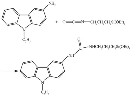
Scheme 1Synthesis route for compound Cz-Si
ThepreparedCz-Sicontainsacarbazole fragment,which will benefit for the hole transporting, and a reactive terminal group-Si(OEt3),rendering the possibility for chemical modification on the ITO surface.When ITO is soaked in the solution of Cz-Si/ CHCl3,the-Si(OEt3)group of Cz-Si would react with -OH group on the ITO surface,thus resulting in a self-assembly monolayer on the ITO surface.The SAM modification procedure is given in Scheme 2:
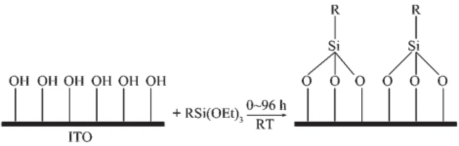
Scheme 2Procedure for SAM modification of ITO (RSi(OEt)3=Cz-Si)
Compared with-SiCl3group,which could react with the OH group on ITO rapidly[16-19],the reactionactivity of the group-Si(OEt3)is relatively lower,thus the SAM modification procedure with Cz-Si should take relatively long time at RT,or need higher temperature.Although there is a little time-consuming,it renders the advantage that the SAM modification could be carried out at ambient atmosphere without anyprotection,offeringthefacilitationforthe modification operation.In this work we investigated the effect of different periods of processing time(0~96 h)on the SAM at RT.It would lead to an undesirable SAM on ITO while the processing time is too short or too long,i.e.,the coverage of SAM on ITO would be imperfectwhileitistooshortandtheselfcondensation(due to the favorable energy of formation for the Si-O-Si linkage)would take place while it is too long.The modified ITO with a certain period SAM processing time is denoted as ITO/SAM(x)h in the following text.
To confirm that Cz-Si is chemically grafted onto the ITO surface,the bare ITO and ITO/SAM(24)h surfaces were characterized by XPS(Fig.1).As shown in Fig.1,the signal of In3d3/2,5/2and Sn3d3/2,5/2decreases after SAM modification,while that of Si2s,2p increases obviously,which is resulted from the coverage of Cz-Si on the ITO surface,indicating successful grafting of Cz-Si onto ITO surface,because all the physically absorbed residues are removed.
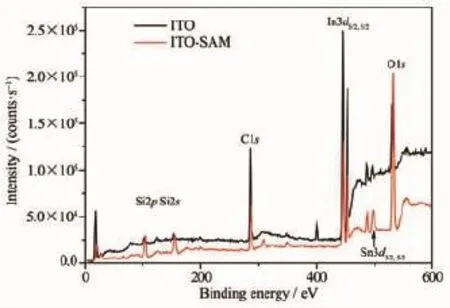
Fig.1 XPS spectra of the bare ITO(black line)and SAM modified ITO(red line)
ITOishighlyhydrophilicwithaheavily hydroxylated inorganic surface,while the organic HTLs(e.g.,TPD and NPB)are hydrophobic.This huge difference is disadvantageous for the growth and stability of the organic film.It is argued that a primary failure mechanism arises from significant mismatches of interfacial surface energy within the heterostructures[22].This large disparity insurface energies promotes the loss of ITO/HTL interfacial integrity,leading to chemical degradation and erosion of emissive efficiency of the device.So tuning the surface energy of the ITO(qualitatively indexed by advancing aqueous contact angle data)would result in positive effect on the performance of the OLEDs. Insertion of SAM between ITO and HTL layer would increase the hydrophobility of the ITO surface,thus eliminating the inorganic/organic interfacial disparity at the ITO/HTL interface.The contact angles for bare ITO and ITO/SAM(24)h in our work are 31°and 73°,respectively(Fig.2).This result indicates that the SAM increases the hydrophobility of ITO surface remarkably,and offers an integrated ITO/organic layer interface.The contact angle is reasonably expected to be higher when the soaking time of ITO in the Cz-Si solution increases,because it increases the coverage ratio of the Cz-Si on ITO.

Fig.2 Aqueous contact angle of bare ITO(left)and SAM modified ITO(right)
The energy level of the active material Cz-Si is crucial to the hole injection of the device.The HOMO level of Cz-Si by CV is shown in Fig.3.The oxidation potential(Eox)is 1.3 eV.According to the equation[23]: HOMO=-(Eox+4.8)eV,the calculated HOMO level of Cz-Si is-6.1 eV.In fact,the HOMO level of Cz-Si is lower than that of NPB(-5.4 eV)[24-25],which is disadvantageous for the hole injection.Considering that the electron transporting rate of the electron transporting layer is lower than the hole transportingrate of the hole transporting layer,the restriction of hole injection to some extent will benefit for the balance of the carriers,which is pivotal for the enhancement of the device performances and stability.

Fig.3 Cyclic voltammetry curve of Cz-Si
To investigate the effect of Cz-Si-SAM on the device performances,a series of devices with the classical structure were fabricated:
DeviceⅠ:ITO/SAM(x)h/NPB(50 nm)/Alq3(60 nm)/LiF/Al
DeviceⅡ:ITO/NPB(50 nm)/Alq3(60 nm)/LiF/ Al
where x is the SAM processing time.When x>20, DeviceⅠshows remarkable performance improvement compared with DeviceⅡ.While when x≤12,the device exhibits similar performance to that of the unmodified counterpart.Whenx=38,the device achieves the best performance.The turn-on voltage (Von),maximum brightness(Bmax)and maximum current efficiency(Effmax)of this device are 5.5 V,21 464 cd· m-2and 5.0 cd·A-1,respectively,while that of the unmodified device(DeviceⅡ)are 6.1 V,12 715 cd· m-2and 3.2 cd·A-1,respectively.The enhancement of brightness and efficiency is 69%and 56%,respectively. On the other hand,device performances decrease gradually with further increasing processing time.The performance of the modified device and unmodified one is listed in Table 1.The V-J-B characteristics of the device ITO/SAM(38)h/NPB(50 nm)/Alq3(60 nm)/ LiF/Al and DeviceⅡ(inset)are shown in Fig.4.

Fig.4 V-J-B characteristics of the device ITO/SAM(38) h/NPB(50 nm)/Alq3(60 nm)/LiF(1.0 nm)/Al; Inset(the V-J-B characteristics of the DeviceⅡ)

Fig.5 Efficiency-Current density characteristics of the modified(SAM procesing 12~48 h)and unmodified(0 h)devices

Table 1Performance of the devices with modified ITO(SAM processing time from 12 to 48 h) and unmodified ITO as anodes
Fig.5 shows the current density-efficiency curves of the devices.The devices with ITO/SAM anodes show much higher efficiency than the unmodified ones.The modified ones could endure higher current density,exhibiting relatively high efficiency under high current density,e.g.,the efficiency of the devicebased on ITO/SAM(38)h is 2.2 cd·A-1at 800 mA· cm-2,while that of the unmodified device decreases to 0.3 cd·A-1.The brightness of the devices is enhanced dramatically also after the ITO modification with SAM,as shown in Fig.6.

Fig.6 Brightness-Current density characteristics of the modified(SAM processing 12~48 h,12~48 h) and the unmodified standard devices
Considering that Cz-Si contains the carbazole unit,theSAMisspeculatedtopossesshole transportingability.Theothertwodeviceswere fabricated with thinner NPB layers:
DeviceⅢ:ITO/SAM(40 h)/NPB(40 nm)/Alq3(60 nm)/LiF(1.0 nm)/Al
DeviceⅣ:ITO/NPB(40 nm)/Alq3(60 nm)/LiF(1.0 nm)/Al
The main performance of these two devices is listed in Table 2.As our speculation,the Cz-Si SAM layer could act as HTL partly,leading to relatively favorable performances when the thickness of NPB is appropriatelyreduced.Ontheotherhand,the unmodified counterpart displays obviously lower EL performances.The brightness and efficiency of DeviceⅢimprove 256%and 140%respectively,when compared with that of DeviceⅣ.
Fig.7 shows the efficiency-current density curves of DeviceⅢand DeviceⅣ.The efficiency of DeviceⅢincreasesrapidlyunderlowcurrentdensity, indicating high combination probability of holes and electrons,while the efficiency of DeviceⅣincreases slowly under the same condition.This result indicates thattheSAMmodificationimprovesthecarrier balance of the device effectively.

Fig.7 Efficiency-Current density characteristics of the DeviceⅢ(modified)and DeviceⅣ(unmodified)devices
The operation stability of the device could also be improved remarkably after ITO SAM modification. The device with ITO/SAM anode shows better stability than the unmodified counterpart when the devices are without encapsulation in the ambient atmosphere for 30 d.Fig.8 shows the V-J-B curves of DeviceⅤand thatofitscounterpartDeviceⅥ(inset).The structures of these two devices are listed as follows:
DeviceⅤ:ITO/SAM(60 h)/NPB(40 nm)/Alq3(60 nm)/LiF(1.0 nm)/Al
DeviceⅥ:ITO//NPB(40nm)/Alq3(60nm)/LiF(1.0 nm)/Al
As shown in Fig.8,the V-J-B characteristics of Device V keep well.The maximum current density (Jmax)and Bmaxof Device V maintain at about 600 mA· cm-2and 5 300 cd·m-2respectively.In contrast,the Jmaxand Bmaxof DeviceⅥdecline to 50 mA·cm-2and 520 cd·m-2respectively,and the device should be operated at high working voltage.This result indicates that the SAM modification could improve the device stability effectively,which might be ascribed to the elimination of disparity in surface energies at the ITO/ HTL interface after SAM modification.

Table 2Performance of deviceⅢ(modified)and DeviceⅣ(unmodified)

Fig.8 V-J-B characteristics of DeviceⅤand DeviceⅥ(inset)after being kept in air for 30 d
The effect of the SAM on the device performance could be understood in terms of hole injection barrier, interface integrity and surface roughness.Firstly,from the view of the energy level,insertion of Cz-Si SAM layer between ITO and HTL will increase the hole injection barrier,because the HOMO level of Cz-Si is lower than that of NPB,which results in lower hole injection efficiency.On the other hand,the image force[26]resulted from molecular SAM could enhance the hole injection efficiency.These two reverse effects exist simultaneously within the heterostructure,and the observed result is the competing consequence. From our results,the image force effect is stronger than that of the energy level,because the Vonof the devices decreases a little.But the superiority is small because the decrease of Vonof the device is small after modification(Table 1 and 2).Secondly,the chemically grafted SAM film could eliminate the disparity at the ITO/HTL interface,to improve the growth quality of the organic film and the stability of the device.Our aqueous contact angle results show that the ITO/SAM is nearly hydrophobic as the organic HTL(e.g.,NPB[22]).This enhanced interfacial integrity will benefit for hole injection and film uniformity,offering better device performance and stability.Thirdly,thesurfaceofITOcouldbe smoothed after modification with SAM,leading to pinhole-free organic functional layers and reduced leak current.Furthermore,the SAM layer could prevent In3+ion migration from ITO anode to the emitting layer[27],improving the device performance. Although enhanced device performance is achieved by ITO SAM modification,the quality of the SAM should be controlled rationally.Because the HOMO level of Cz-Si is relatively low,Cz-Si layer with excessive thickness(e.g.,formation of multilayer due to selfcondensation from too long SAM processing time) would result in decline of enhancement rate for the efficiency and the brightness of the device as reflected in Table 1.The performance of the devices declines after the SAM processing time exceeding 38 h,which might be attributed to the over thickness of the Cz-Si film on the ITO surface.
3 Conclusions
AnovelorganosilaneCz-Siwasdesigned, synthesized and used for the active material for SAM modification on ITO surface.Due to the stability of Cz-Si,the processing of the SAM modification is simple and convenient,which could be carried out in ambientatmospherewithoutanyprotection.By controlling the formation of the SAM layer,a series of electroluminescenct devices with ITO/SAM or bare ITO as anodes were fabricated,and the devices with ITO/SAM anodes show remarkable improved performance when compared with their unmodified counterparts.Best device performance is achieved when ITO/SAM(38 h)is used as anode,and the Von,Bmaxand Effmaxof this device are 5.5 V,21 464 cd·m-2and 5.0 cd·A-1,respectively.The device stability is improved also after ITO modification with SAM.The device with ITO/SAM anode exhibits better performance than its unmodified counterpart.
Acknowledgments:Theauthorsaregratefultothe financial aid from the National Natural Science Foundation of China(Grant No.21221061),the National Key Basic Research Program of China(No.2014CB643802),the Youth Innovation Promotion Association of Chinese Academy of Sciences(No. 2013150),andJilinProvincialScienceandTechnology Development Program of China(No.20130522125JH).
References:
[1]Kim J S,Cacialli F,Cola A,et al.Appl.Phys.Lett.,1999, 75:19-21
[2]Li C N,Kwong C Y,Djurišic'A B,et al.Thin Solid Films, 2005,477:57-62
[3]Helander M G,Wang Z B,Qiu J,et al.Science,2011,332: 944-947
[4]Lee S T,Wang Y M,Hou X Y,et al.Appl.Phys.Lett.,1999, 74:670-672
[5]Cui J,Huang Q,Veinot J G C,et al.Adv.Mater.,2002,14: 565-569
[6]Brown T M,Kim J S,Friend R H,et al.Appl.Phys.Lett., 1999,75:1679-1681
[7]Koch N,Kahn A,Ghijsen J,et al.Appl.Phys.Lett.,2003, 82:70-72
[8]Tang J X,Li Y Q,Hung L S,et al.Appl.Phys.Lett.,2004, 84:73-75
[9]Hsiao C C,Chang C H,Jen T H,et al.Appl.Phys.Lett., 2006,88:033512
[10]Luo J X,Xiao L X,Chen Z J,et al.Appl.Phys.Lett.,2008, 93:133301
[11]Zhang H M,Fu Q,Zeng W J,et al.J.Mater.Chem.C, 2014,2:9620-9624
[12]Zhou L,Zhuang J Y,Tongay S,et al.J.Appl.Phys.,2013, 114:074506
[13]Chu T Y,Chen J F,Chen S Y,et al.Appl.Phys.Lett., 2006,89:053503
[14]Hotchkiss P J,Jones S C,Paniagua S A,et al.Acc.Chem. Res.,2012,45:337-346
[15]Kim D H,Chung C M,Park J W,et al.Ultramicroscopy, 2008,108:1233-1236
[16]Jonathan G C,Veinot,Marks T J.Acc.Chem.Res.,2005, 38:632-643
[17]Huang Q,Li J,Evmenenko G A,et al.Chem.Mater.,2006, 18:2431-2442
[18]Huang Q,Evmenenko G A,Dutta P,et al.J.Am.Chem. Soc.,2005,127:10227-10242
[19]Yan H,Lee P,Armstrong N R,et al.J.Am.Chem Soc., 2005,127:3172-3183
[20]Huang Q,Cui J,Yan H,et al.Appl.Phys.Lett.,2002,81: 3528-3530
[21]Huang Q,Evmenenko G,Dutta P,et al.J.Am.Chem.Soc., 2003,125:14704-14705
[22]Wu Q H.Crit.Rev.Solid State,2013,38:318-352
[23]HUANG Chun-Hui(黄春辉),LI Fu-You(李富友),HUANG Wei(黄维).Introduction to Organic Light-emitting Materials and Devices(有机电致发光材料与器件导论).Shanghai: Fudan University Press,2005:111
[24]Cheng G,Zhang Y F,Zhao Y,et al.Appl.Phys.Lett., 2005,87:013506
[25]Shi J and Tang C W.Appl.Phys.Lett.,2002,80:3201-3203
[26]Tutis E,Bussac M N,Zuppiroli L.Appl.Phys.Lett.,1999, 75:3880-3882
[27]Wong K W,Yip H L,Luo Y,et al.Appl.Phys.Lett.,2002, 80:2788-2790
Indium Tin Oxide Anode Self-Assembled Monolayer Modification for Device Performance Improvement of Organic Light-Emitting Diodes
DENG Rui-PingZHOU Liang*LI Lei-JiaoZHANG Hong-Jie*
(State Key Laboratory of Rare Earth Resource Utilization,Changchun Institute of Applied Chemistry, Chinese Academy of Sciences,Changchun 130022,China)
A novel alkoxysilane(Cz-Si)was synthesized and used as an active reagent for self-assembled monolayer(SAM)modification on indium tin oxide(ITO)surface.The as-prepared Cz-Si could modify the ITO surface successfully under the mild atmosphere without any protection,offering simple and easy experimental operation.To investigate the effect of SAM modification on the device performances,based on ITO/SAM anodes, a series of organic light-emitting diodes(OLEDs)were fabricated:ITO/SAM(or unmodified)/NPB(40~50 nm)/Alq3(60 nm)/LiF(1.0 nm)/Al.The devices show improvement compared to their counterparts with bare ITO anodes. The improvement could be attributed to the modulating of the electronic energy,surface roughness and interface integrity at the ITO/hole transporting layer(HTL)interface by SAM modification.
ITO modification;self-assembled monolayer(SAM);organic light-emitting diodes(OLEDs)
O614.33+8
A
1001-4861(2015)09-1839-08
10.11862/CJIC.2015.242
2015-05-29。收修改稿日期:2015-07-17。
科技部“973”计划(No.2014CB643802),国家自然科学基金创新群体(No.21221061),中国科学院青年创新促进会项目(No.2013150),吉林省科技发展计划项目(No.20130522125JH)资助项目。
*通讯联系人。E-mail:hongjie@ciac.ac.cn,zhoul@ciac.ac.cn
