无线激光通信协议的设计
2011-11-06赵丽丽王挺峰孙文涛
赵丽丽,王挺峰,孙文涛,郭 劲
(1.中国科学院长春光学精密机械与物理研究所激光与物质相互作用国家重点实验室,吉林长春130033; 2.中国科学院研究生院,北京100039)
1 Introduction
With the maturity and development of laser diode technology,the photoelectric conversion efficiency of laser devices has been greatly improved,and the driving voltage bump has been greatly reduced.Therefore,people consider a new generation of laser communication system as an ideal choice.The Free Space Optical(FSO)communication is one of communications which uses the optical band as its carrier through the space.It not only includes communication in deep space among Geostationary Earth Orbit(GEO)satellites and Middle Earth Orbit(MEO)satellites,but also includes the communication among terrestrial terminals.Comparing the laser communication with existing wired and wireless communications,the FSO communication system has the characteristics of higher bandwidth,higher speed and higher reliability,which can be immune to external electromagnetic interference[1-2].
Over the past several decades,optical fiber system has developed rapidly.The laser communication systems mainly include optical fiber systems whose transmission medium is the optical fiber owing to its relatively simple channel model and low power attenuation of the laser beam.Combined with the radio communication system,the fiber optic systems have become the most important communication technology.However,the channel model of the FSO system is much more complicated,because the laser carrier is easily influenced by the laser propagation direction and the power loss[2-6].
Considering the complexity of the channel model of the atmosphere and its significant influence on the system reliability,it is much more difficult to design an FSO system than an optic fiber system.So we can understand why the development of the FSO system is much slower than that of the optic fiber system[7-9].Both the hardware design and the software design have to be optimized for the atmospheric channel to design an FSO system.Considering the characteristics,the small wireless laser communication systems and hardware system developed for the software protocol are designed.
2 Hardware specifications
2.1 Hardware design
The design of the hardware platform is a laser pointto-point full-duplex wireless communication system,and each optical transceiver consists of a transmitter and a receiver form.The role of the transmitter is to send data to be encoded,serialized and converted into optical signals,and then launch it into the space;and the role of the receiver is to receive the optical signal for photo-electric conversion,deserializing and decoding.

Fig.1 Constitution diagram of hardware platform
The platform of the FSO communication system mainly consists of a Field Programmable Gate Array(FPGA),a laser driver,a laser diode,pin photodiodes,signal amplifiers and optical antennas.The FPGA chip interfaces the communication platform to outer systems and utilizes the function of our transceiving protocol.The entire constitution diagram of our hardware platform is as shown in Fig.1,in which the shaded blocks are related to our protocol.
For the transmit channel,the FPGA receives data to be transmitted to the other FSO terminal through a 8-bit parallel port,and then sends the input data to the transmitting protocol module inside the FPGA.The buffered input data in a First In,First Out(FIFO)is coded to the right format for FSO and hardware platform,then serialized and output to the laser driver module whose function is to transform the received voltage signal into a drive current to drive the laser diode,including the bias current and the modulation current.Low Voltage Differential Signaling(LVDS)bus is the interface between the FPGA and the laser driver module which could improve the transmission rate.The modulated optical signal from laser driver is coupled into the fiber,and then emitted from the optical antenna to outer atmosphere.
For the receive channel,it performs inverse procedure of the transmitting system.The optical signal collected by the optical antenna is coupled to the fiber and then to the pin detector,in which the signal is transformed into the weak current proportional to the laser power.The weak current generated by the pin detector will be sent to the amplifier procedure,which includes the transimpedance preamplifier and the limiting amplifier[9-10].The later amplifies the voltage signal from the preamplifier and qualifies it to fit its connection to the FPGA chip through an LVDS interface.The FIFO data in the receiver buffers received data and an external processor can read out the data through the 8 bit parallel bus from inside the FPGA.The receiving protocol in the FPGA continuously samples the serial data stream from the limiting amplifier.Once it receives useful data or a command,it will deserialize the command or the data,decodes it,and send it to the receiver FIFO or execute it if it is a command.

Fig.2 Schematic diagram of laser driver module
2.2 Laser driver module
The schematic diagram of laser driver module is shown in Fig.2.The TX_DISABLE is used to disable the drive current of the laser driver.The laser output will be disabled when TX_DISABLE is high until it is asserted low.TX_FAULT is a hardware error indicator.The driver will shut down the drive current when the defined conditions happen.To recover from this error state,it needs to be a toggle of the TX_DISABLE pin or the power supply.Although the TX_FAULT and the TX_DISABLE are all connected to the FPGA,it is indicated that the working state can be controlled manually by the operator.TX_FROM_FPGA+and TX_FROM_FPGA-are the differential inputs through the LVDS interface that connects the FPGA.Some of the resister and capacitor values are determined by the parameters of the laser driver.
The hardware platform uses MAX3735A as the laser driver chip.The data rate is from 155 Mbps to 2.7 Gbps and the supply voltage is 3.3 V.The data input interface is a LVDS differential serial interface,which is connected with the FPGA and dedicated to the high-speed serial data transmission.MAX3735A can provide 10-60 mA modulation current and 1-100 mA programmable bias current for laser programmably.In addition,MAX3735A also has the functions of output control,fault detection,output power detection and automatic power control.
The mechanism of the driver chip's Automatic Power Control(APC) feature includes the chip which monitors the average feedback current.Since the current of the PD is proportional to the optical power,the average current of the PD is proportional to the average optical power.If the differential voltage between the IN+and IN-pin of the MAX3735 chip is always logical“1”,the optic power of the laser driver is supposed to be continuously in high power status.However,when the average current of the PD becomes higher,the chip will reduce the laser driver's bias current to make the average PD current stable on the fixed value.
2.3 Signal transforming and amplifying module
The signal transforming and amplifying module is shown in Fig.3.The PD_DISABLE is used to stop the limiting amplifier from transmitting data to the FPGA.The PD_LOS is used to indicate the losses of high or low received optical powers.Although both the PD_LOS and the PD_DISABLE are connected to the FPGA,they are neither controlling nor controlled by transceiving protocol.Considering that our protocol has error checking and failure recovery mechanism,it is just controlled by the operator.The REC_TO_FPGA+and REC_TO_FPGA-are the differential outputs through the LVDS interface.
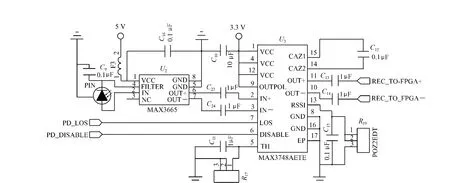
Fig.3 Diagram of signal transforming and amplifying module
Through low-frequency feedback,the DC cancellation loop can remove the DC component of the pin current.It brings the baseline excursion problem and reduces the pulse-width distortion on large input signals.When long continuous zeros appear in the data stream,the MAX3665 detects no AC component and the DC cancellation loop will reject all useful signals. On thatcondition, the outputof MAX3665 will be zero and the limiting amplifier will generate a loss-of-signal error while the pin detector has already detected the optical signal.So the same as in the laser driver module,the transceiving protocol should guarantee that the possibility of both high optical power and low optical power can meet the requirement of the preamplifier.
3 Protocol design
The transceiving protocol for the FSO communication system consists of the transmitting protocol and the receiving protocol.Communication protocol overview is shown in Fig.4.Three blocks are respectively the transmitting protocol module,the receiving protocol module and a PLL generate clocks with the same frequency for the two protocol modules.From the outside of the protocols,the transmitting protocol module looks like a write-only FIFO and a serial output bus,while the receiving protocol module looks like a read-only FIFO and a serial input bus.When this protocol is used in the FSO system,you can operate the system once you operate the FIFO.That is why we call it a transparent protocol.The two protocol modules are not isolated from each other while connected by four signals“stoptrans”,“stoprec”,“startrec”and a clock signal“clk12”is at the transmitter side.
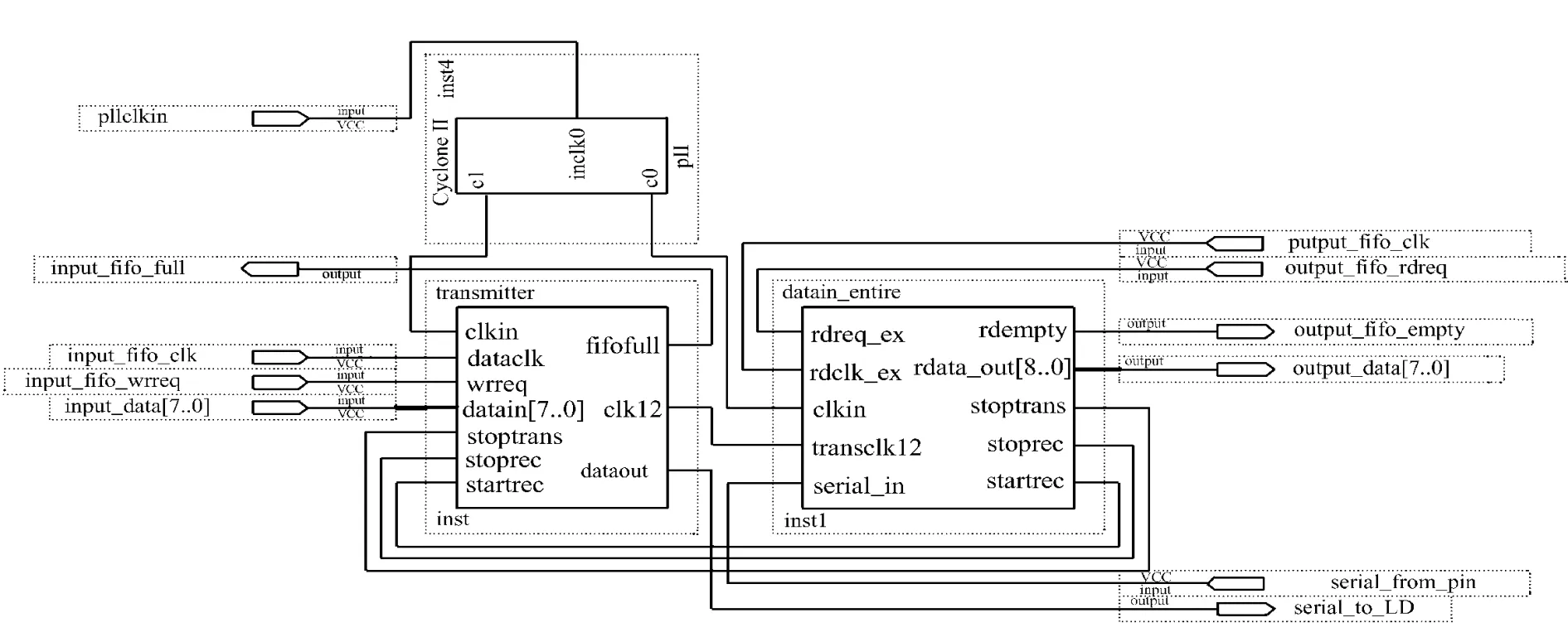
Fig.4 Diagram of communication protocol overview
The protocols in two terminals have to communicate with each other.In other words,optical signal not only transmits users'information but also communicates information between the two terminals.The“stoprec”signal is generated by the receiving protocol to inform the transmitting protocol.As soon as the transmitting protocol receives the“stoprec”signal,it stops transmitting user information but transmits a“stoprec”command to inform the other terminals.The“stoptrans”signal is interpreted by the receiving protocol from received information.It implies that other terminals are not readily to receive data.The“clk12”is not a command signal,which aligns other three commands with signals of the transmitting module.
3.1 Transmitting protocol design
The transmitting protocol are composed of 6 blocks,including the clock generator,the transmitter FIFO,the coder,the register group,the output management unit,and the serializer.The transmitting protocol is shown in Fig.5.
The clock generator is used for generating 3 necessary clocks needed by the transmitting protocol,and guarantees that these 3 clocks are well aligned to meet the timing requirement for all blocks.The FIFO module acts as a buffer of input data and it also makes the transmission operation easier.

Fig.5 Diagram of transmitting protocol
The coding block has two sub-blocks.One is completing a 4B6B coding and the other is transforming the 8 bit input data into a satisfied format that meets the requirement of the hardware platform and reliability.In the encoder module,the 8 bit input data are read out and divided into two 4 bit groups,the higher bits and the lower bits,then the two groups are put into the coding procedure where coded group is available for the next step.The register group store command codes for the communication between the two terminals.Under the control of the output management unit,one of the register groups is selected to be serialized out to the laser driver.The output management unit is the core of the transmitting protocol.It determines the content of information to be transmitted by analyzing the protocol's working state and receiving command from the other terminal.
When there is neither data nor command to transmit,the register group shifts the “regout[5:0]”to the power-modify register containing the value of“111000”,then the“dout”of the serializer block will continuously output the data stream of“111000”until data or command are to be transmitted.In this way we can avoid the baseline excursion happening.What's more,the power-modify stream“111000”could be used as the synchronization signal of the transmitter and the receiver.
3.2 Receiving protocol design
The receiving protocol diagram is composed of 6 blocks,including the clock generator,the receiver FIFO,the decode block,the streamfilter block,the deserializer block and the exception handle block.The receiving protocol is shown in Fig.6.
The clock generator and the receiver FIFO play the same role as that in the transmitter protocol.While the system starts working,it transmits the power-modify signal.When the streamfilter detects the power-modify signal sequence,it forces the clock generator to synchronize with the sequence and it is also used for synchronization information.As soon as the synchronization finishes,the streamfilter will reset all error flags,the“sper”,the“syncer”,and the“dser”.The deserializing block“parallel”continuously samples the signal stream and send the lower 6 bits to the streamfilter at the receiver side.At last the exception-handle module generates a“startrec”signal to inform the other terminal that the terminal is available for receiving data.

Fig.6 Diagram of receiving protocol
When the other terminal transmits user data,the deserializer samples the data stream and sends the sampled data stream and the sampled 6 bit data group to the streamfielter.Then the steamfilter evaluates the health status of the receiving module.If the streamfilter detects no error,both the FIFO and the decode block will keep working under control.Once a short term or a long term error is detected by the streamfilter,it will shut down the decoder and the receiver FIFO,and inform the exception-handle block of the error state,then the exception-handle block takes steps to inform the other terminal of the error state through the“stoprec”command so as to stop it from transmitting user data.If the terminal in error-state receivesno power-modify signaland keeps receiving error data,the streamfilter will assert the two terminals in an error state or something will go wrong with the atmospheric channel,afterwards it informs the exception-handle block of this situation,so the exception-handle block will send a“stoptrans”command to the transmission block to stop transmitting user data.Finally,when two terminals get back to the synchronized status,the transmitter transmits the power-modify signal and then enters next cycle.

Fig.7 Diagram of internal logic state when fTis 50 MHz,and fRis 51.67 MHz
4 Result of emulator
We have done some experiments to test the reliability of the protocol.Fig.7 shows the working waveform whenfTis 50 MHz,andfRis 51.67 MHz,while in Fig.8,fTis 50 MHz,andfRis 48.44 MHz.

Fig.8 Diagram of internal logic state when fTis 50 MHz,and fRis 48.44 MHz
In Fig.7,we can see the internal logic state when the protocol is in ordinary operation and in Fig.8,we can see the internal logic state when the protocol recovers from an error.The waveform is the actual working waveform which is read from Signal-Tap II logic analyzer embedded inside FPGA.The“sgnltpclk”is logic analyzer sampling clock;the“crntclk”is global clock number;the“nxtclk”is the next global clock number to be used;the“smplclk”is the sampling clock in actual use generated by“Clock Generation Module”;the“smplddata”is the sampled data.
From the results we know that the protocol can work well on a certain data rate scale,besides that it could recover rapidly after fatal errors.However,once the data rate is rising,the system will become unstable,and it even fails to transmit the right content or recover from error.Now we realize that there is a little flaw when designing the PCB arraying,which makes it bring in overshooting of the high speed signal.
5 Conclusions
In this paper,we introduce a new transceiving protocol with a simple structure and a low cost for the FSO communication system which consists of the transmitting protocol and the receiving protocol.When there is data transmission between the two terminals,the transmitting protocol buffers the data,codes the data and then serializes the data.The serialized data is transmitted to the receiver.On the receiverside,the protocoldeserializesthe data stream,decodes the data and puts the received data into the FIFO.The error state of the received data stream is used to determine the availability of the channel state.In the case of different types of errors,the protocol takes reasonable action to ensure reliable data transmition.So we can take a conclusion that the protocol has the ability to recover from error by filtering and monitoring the received data.Once an error happens,the streamfilter and the exception-handle module can detect the error and take steps to recover from the error.The analysis of theory and experiments proves that the presented protocol is a working solution in the field of FSO at a rate of 40 Mbit.
Reference:
[1]KE X Z.Introduction to Wireless Laser Communications[M].Beijing:Beijing University of Posts and Telecommunications Press,2004.
[2]WANG H Y.Research on free space optical communication system and its major components[D].Tianjin:Tianjin University,2005.
[3]ZHENG Y G,LI B.The applied development of optical communication in free space[J].Wireless Optical Communication,2007(7):52-53.
[4]WANG J.The technology research and development review of free-space optical communication[J].Opt.Technology,2005(31):259-262.
[5]CHEN Y B,ZHAO S H.The technology research and prospects of free-space optical communications[J].Opt.Communications,2003(4):11-15.
[6]ZHANG W T.Technology and development of free-space laser communication[J].J.Quantum Electronics,2003(3):269-272.
[7]KIM I I,MCARTHUR B,KOREVAAR E.Comparison of laser beam propagation at 785 nm and 1550 nm in fog and haze for optical wireless communications[J].SPIE,2001,4214:26-37.
[8]YU S Y,MA J.The technology trends analysis of Free-space laser communications[J].Wireless Opt.Communication,2004(12):47-50.
[9]BLOOM S,KOREVAAR E,SCHUSTER J,et al..Understanding the performance of free-space optics[J].J.Opt.Networking,2003(2):178-200.