Effects of irradiation on superconducting properties of small-grained MgB2 thin films
2023-12-15LiLiu刘丽JungMinLeeYoonseokHanJaeguSongChorongKimJaekwonSukWonNamKangJieLiu刘杰SoonGilJungandTusonPark1
Li Liu(刘丽), Jung Min Lee, Yoonseok Han, Jaegu Song, Chorong Kim,Jaekwon Suk, Won Nam Kang,†, Jie Liu(刘杰), Soon-Gil Jung, and Tuson Park1,,¶
1Center for Quantum Materials and Superconductivity(CQMS),Sungkyunkwan University,Suwon 16419,Republic of Korea
2Department of Physics,Sungkyunkwan University,Suwon 16419,Republic of Korea
3Institute of Modern Physics,Chinese Academy of Sciences(CAS),Lanzhou 730000,China
4School of Nuclear Science and Technology,University of Chinese Academy of Sciences(UCAS),Beijing 100049,China
5Korea Multi-purpose Accelerator Complex,Korea Atomic Energy Research Institute,Gyeongju,Gyeongbuk 38180,Republic of Korea
6Department of Physics Education,Sunchon National University,Suncheon 57922,Republic of Korea
Keywords: MgB2 films,grain boundaries,flux pinning,low-energy ion irradiation
1.Introduction
MgB2has tremendous potential for practical applications owing to its excellent superconducting properties.For instance,the superconducting critical temperature(Tc)of MgB2is approximately 40 K, which makes it a promising material for use in liquid-helium-free apparatus.[1]Its high upper critical field(Hc2)makes MgB2a suitable alternative for commercial superconductors in high-field magnet applications.[2-4]Moreover, from the aspect of radioactivity, MgB2is one of the promising materials in neutron irradiation environment,such as fusion reactor,because of its shorter half-life of the induced activity than Nb-based superconducting alloys.[5]Grain boundaries (GBs) in MgB2function as a strong pinning site owing to its large coherence length (ξ).In addition, no weak link behavior across GBs is observed in MgB2, which is in contrast to the weak link behavior in high-Tccuprate superconductors.[6]Therefore,a kilometer-long MgB2superconducting wire used in real systems can be fabricated using a simple powder-in-tube technique, thus considerably reducing the manufacturing cost.[7,8]
The high current-carrying capability for superconductors necessary for practical applications in magnetic field environment can be achieved by introducing artificial defects.[9]Particle irradiation is a suitable method for producing defects in superconducting materials and has been successfully used in roll-to-roll 80-m long YBa2Cu3O7-δcoated conductors.[10,11]The effect of irradiation on MgB2has been widely studied since it discovered in 2001.[12]Neutron has been suggested as a potential irradiating source for MgB2due to the large thermal neutron capture cross section of the10B atom(∼20%in natural B), which causes defects through the10B(n,α)7Li reaction.[13]The self-shielding effect of the10B atoms induces inhomogeneous defects around the surface.However, homogeneous damage can be achieved by replacing10B with11B isotope.[14,15]
The GBs in metals are known to act as an effective sink for irradiation-induced defects.[16]Irradiation-induced defects, such as vacancies and interstitials, including injected ions can easily migrate into the GBs because the defect diffusion barrier near GBs is considerably lower than the defect diffusion barrier within the grains.[17,18]Moreover, the process of absorbing irradiation-induced defect clusters around GBs has also been observed byin situtransmission electron microscope.[19,20]Hence,the radiation tolerance of nanocrystalline materials is larger than that of coarse-grained samples,which can be improved as the density of GBs increases.[21,22]
Considering the metallic characteristics of MgB2superconductors,[23]it can be assumed that ion irradiation has a significant influence on grain boundary pinning of MgB2with small grain sizes.In this study, we irradiated 120-keV Mn ions on MgB2thin films with nanoscale grain sizes.The critical current density(Jc)of the pristine MgB2samples was rapidly decreased with the increase in magnetic field owing to a good inter-grain connectivity.However, the field performance ofJcof the irradiated films was significantly improved with the change of the flux pinning mechanism from weak to strong pinning.The scaling behavior of the flux pinning is consistent with the dominance of surface pinning in the irradiated films, underpinning that GBs in MgB2can act as an effective sink of irradiation-induced defects.
2.Material and methods
Thec-axis-oriented MgB2thin films with grain sizes of approximately 122 nm and 140 nm were fabricated using a hybrid physical-chemical vapor deposition(HPCVD)system,and the details of the fabrication condition and quality of films were described everywhere.[24-26]Thec-cut Al2O3substrate of 10 mm×10 mm in size was placed on the susceptor filled with 99.99% purity Mg pieces.The carrier gas was H2at a flow rate of 80 sccm,and the susceptor was heated to 700◦C in a total pressure of 100 Torr(1 Torr=1.33322×10²Pa).Subsequently,5%B2H6in H2gas(20 sccm)was introduced into the chamber to grow the MgB2thin films.The growth rate of the films was approximately 2.5 nm/s.
Ion irradiation was performed at the Korea Multi-purpose Accelerator Complex (KOMAC).The prepared MgB2films were cut into several pieces for irradiation at each fluence,and each MgB2film with thicknesses of 250 nm (MB250)and 430 nm(MB430)were irradiated at room temperature using Mn ions with a beam energy of 120 keV and fluences of 1×10¹³(1E13),5×1013(5E13),and 1×10¹⁴(1E14)ions/cm2.The direction of the incident ions was tilted by 7◦from thecaxis to minimize the channeling effect.The damage events produced in the MgB2thin films by 120-keV Mn ions were determined using the Monte Carlo simulation program, the stopping and range of ions in matter(SRIM).[27]
The crystal phases and orientations of the prepared films were checked by x-ray diffraction (XRD), and average grain sizes of the films were evaluated by counting the number of grains in the area through the surface morphology observed by scanning electron microscopy (SEM).The zero-field-cooled(ZFC)and field-cooled(FC)dc magnetization(M)as well as magnetization hysteresis (M-B) loops were measured by using magnetic property measurement system (MPMS, Quantum Design) equipped with a 5-T superconducting magnet.The direction of the magnetic field was parallel to thec-axis direction of the film.TheJcvalue was calculated from theM-Bloops using the Bean critical-state modelJc=15∆M/r,where ∆Mis the width of theM-Bloops per volume(in units of emu/cm3)andris the radius corresponding to the total area(S)of the film surface,i.e.,S=πr2.[28,29]
3.Results and discussion
The displacements per atom(dpa)produced in the MgB2by 120-keV Mn-ion irradiation with fluences of 1E13,5E13,and 1E14 ions/cm2was simulated using the transport of ions in matter(TRIM)code in the SRIM software,[27,30]as shown in Fig.1.The inset in Fig.1 is a schematic diagram of the MgB2thin film with a thickness of 250 nm (MB250) after 120-keV Mn-ion irradiation,divided into two regions,namely irradiated and unirradiated regions.The thickness of the irradiated region(tD)was determined at the dpa=0.001 because this value has an impact on the field performance ofJcof MgB2,[31]and thetDfor 1E13,5E13,and 1E14 Mn ions/cm2were approximately 136 nm,160 nm,and 170 nm,as indicated by the arrows in Fig.1.
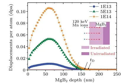
Fig.1.Displacements per atom(dpa)as a function of MgB2 depth,generated by 120-keV Mn-ion irradiation with fluences of 1E13,5E13,and 1E14 ions/cm2.Inset illustrates the schematic view of irradiated and unirradiated areas in 250-nm-thick MgB2 thin film,where the depth of irradiated region(tD)is determined at 0.001 dpa,as indicated by the red solid line and arrows.
Figure 2(a)shows XRD pattern ofθ-2θscan for pristine MB250(MB250-PRI)deposited onc-cut Al2O3substrate,indicating a highlyc-axis orientation.Figure 2(b)is the surface morphology of MB250 observed by SEM.The estimated average grain diameter of MB250 was approximately 122 nm.The magnetic field dependence of critical current density(Jc)of MB250-PRI at 5 K and 20 K is illustrated in Fig.2(c).A large self-fieldJc≈19 MA/cm2at 20 K and its rapid reduction in magnetic field indicate the high quality of the fabricated films.[32]The self-fieldJcis lower at 5 K than at 20 K due to a large flux jump at low fields,as shown in inset of Fig.2(c),which is known as a result of thermomagnetic instability.[33]The flux pinning force density (Fp) as a function of the magnetic field presented in Fig.2(d) reflects the high quality of MB250.Here,Fpwas calculated using the relationFp=Jc×B.The sharp peak ofFp(B)curves at low fields is thought to be caused by the rapid decrease inJc(B)due to the lack of effective pinning sites.[34]
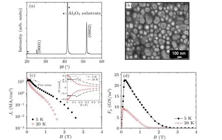
Fig.2.(a)XRD pattern of a θ-2θ scan for MB250-PRI deposited on a c-cut Al2O3 substrate.(b)SEM surface morphology of MB250-PRI where the average grain diameter is approximately 122 nm.(c)Semi-logarithmic Jc-B curves at 5 K and 20 K for MB250-PRI.Inset shows the M-B hysteresis curves at 5 K and 20 K,indicating a presence of large flux jump at 5 K.(d)Magnetic field dependence of volume flux pinning force density(Fp)at 5 K and 20 K for MB250-PRI.
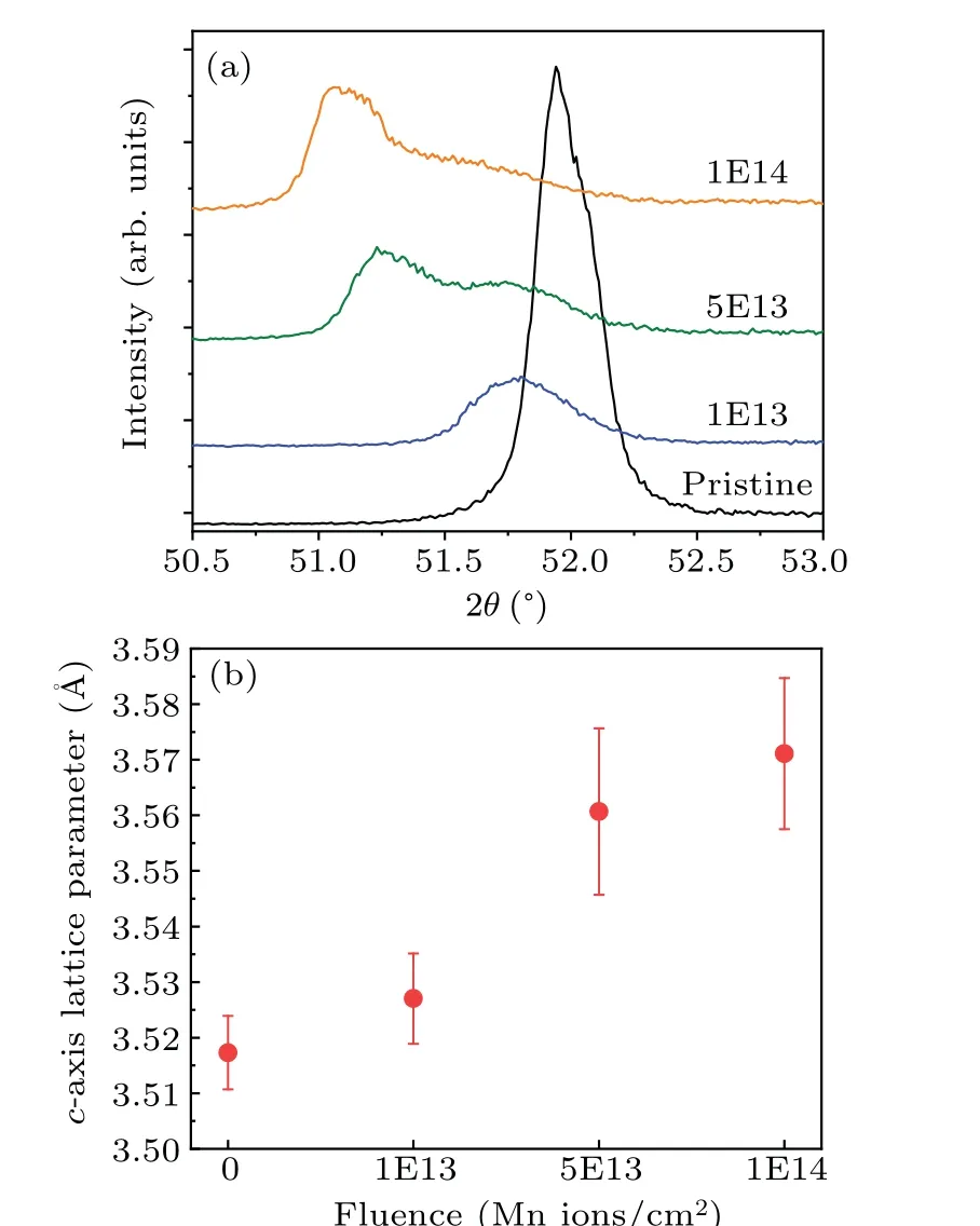
Fig.3.(a) Enlarged view of (0002) peak of MB250 before and after 120-keV Mn-ion irradiation.For the sample irradiated with a fluence of 5×10¹³ ions/cm2, the small broad peak near (0002) peak was related to the remaining unirradiated layer.(b) Changes in c-axis lattice constant of MB250 films as a function of ion fluence.
The changes inc-axis lattice parameter before and after irradiation was characterized by XRD.After irradiation, the(000l) peaks of MB250 shift toward lower angle.For the sake of clarity, an enlarged view of (0002) peak is shown in Fig.3(a).The existence of a broad peak in the sample irradiated at a fluence of 5×10¹³ions/cm2is due to the unirradiated layer, as shown in schematic diagram of Fig.1.Thec-axis parameter calculated from (0002) peak of MB250 increases monotonically with increasing ion fluence,as shown in Fig.3(b),reaching the increment of about 1.53%compared to the pristine sample at a maximum fluence of 1×10¹⁴ions/cm2.
The superconducting transition temperature (Tc) of MB250 was gradually decreased by increasing the amount of irradiated Mn ions.Figure 4 shows the zero-field-cooled(ZFC)and field-cooled(FC)dc magnetization(M)at 5 Oe as a function of temperature for MB250 before and after 120-keV Mn-ion irradiation with fluences of 1E13, 5E13, and 1E14 ions/cm2.The MB250-PRI shows aTcof 38.7 K(corresponding to the transition of 10%in ZFCM(T)curve)with a sharp transition width ∆Tc=1.8 K determined using the transition of 90%to 10%of the superconducting diamagnetic signal in the ZFCM(T) curve, as presented in Fig.4.TheTcgradually decreased whereas ∆Tcincreased as the fluence level increases,and at the highest fluence level of 1E14 ions/cm2,Tcand ∆Tcwere 28.2 K and 6.9 K,respectively.
The reduction ofTcby low-energy ion irradiations can be understood due to the formation of point defects and lattice distortions in MgB2.[35,36]The irradiation-induced disorder can act as impurity scattering centers, thus enhancing inter-band scattering and suppressingTc.[15,37,38]In addition,a decrease in the electron-phonon coupling constant with increasing dpa leads to a suppression ofTc.[39,40]
The magnetic field dependence ofJcat 5 K and 20 K for MB250 before and after 120-keV Mn-ion irradiation is shown in Figs.5(a) and 5(b), respectively.TheJcat low fields is decreased gradually with increasing fluence, associated with a suppression ofTc, and at both temperatures, the magnitude of the self-fieldJcwas suppressed by approximately a factor of 10 at the highest fluence of 1E14 Mn ions/cm2.However,the field performance ofJcwas significantly improved after irradiation.For MB250 irradiated with 1E13 Mn ions/cm2,theJcvalue increased more than 10-fold from approximately 0.02 for the pristine sample to 0.26 MA/cm2at 5 K and 2.4 T.Figures 5(c) and 5(d) plot the flux pinning force density (Fp)as a function of the magnetic field, calculated from theJc(B)curves in Figs.5(a)and 5(b),respectively.For the sample irradiated with 1E13 Mn ions/cm2,Fpat 5 K and 20 K obviously increased at high fields larger thanB>1 T,indicating that the number of effective pinning sites for high fields was increased by irradiation.The significantly decreasedFpat low fields was caused by the decrease inJcwith the suppression ofTcafter irradiation.
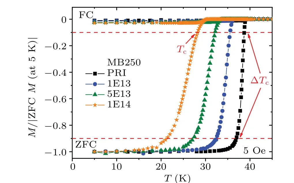
Fig.4.Temperature dependence of ZFC and FC M at 5 Oe for pristine(PRI)and 120-keV Mn-ion irradiated MB250,where the M(T)values were normalized by the absolute ZFC M value at 5 K for comparisons.Superconducting transition width (∆Tc) was defined as the difference between the 10% and 90% transitions of the diamagnetic signal from the normal state and denoted by the arrows with a red color.

Fig.5.Semi-logarithmic Jc-B curves at(a)5 K and(b)20 K for MB250 before and after irradiation.The field performance of Jc is improved by Mn ion irradiation, while the Jc at low fields decreases gradually as the fluence level increases.Magnetic field dependence of Fp is plotted at(c)5 K and(d)20 K.
The scaling behavior of the normalized flux pinning force density(fp=Fp/Fp,max)with respect to the reduced magnetic field (b=B/Birr) for irradiated MB250 was studied, whereFp,maxis the maximumFpandBirris the irreversible magnetic field.Since theJcandFpvalues of type-II superconductors approach zero when the magnetic field is equal toBirr, if theBirrvalue is not close toBc2,Birris more suitable for describing thebvalue to investigate the scaling behavior of flux pinning force.[41,42]TheBirrvalue of the pristine and irradiated MB250 was estimated using the Kramer plot ofJc0.5B0.25∝(Birr-B),[43,44]as described in Figs.6(a)and 6(b).Figures 6(c) and 6(d) show thefpversus bcurve for MB250 at 5 K and 20 K,respectively.
In the scaling law of flux pinning force,fp(b)∝bp(1-b)q, the peak position offp(b) together with parameterspandqis dependent on the characteristics of the dominant pinning source of superconducting samples.[44-46]According to Dew-Hughes(DH)model,thefp(b)peak is located atb=0.2(p=0.5 andq=2) for surface pinning andb=0.33 (p=1 andq=2)for normal point pinning,as shown in Fig.6(c).[46]Thefp(b)curves for MB250-PRI cannot be explained by any pinning models, to the best of our knowledge, because of the low density of effective pinning centers, as discussed in Fig.2(d).However, the flux pinning mechanism of the irradiated MB250 samples showed the predominance of surface pinning.In contrast,since low-energy ion irradiation primarily produces homogeneously distributed point defects caused by nuclear stopping of energetic ions, as depicted in the inset of Fig.6(d),[47]in general,single-crystalline MgB2films showed the dominance of normal point pinning after low-energy ion irradiation.[48,49]
The effect of GBs on the irradiation-induced defects in the relatively thicker MgB2films with a thickness of 430 nm(MB430) was additionally studied in comparison with the thickness of the irradiated regions.The XRD results of the MB430 are shown in Fig.7(a).The(0002)peak clearly splitting into two peaks for the fluence level>1×10¹³ions/cm2due to the presence of thicker unirradiated layer compared to MB250.Thec-axis lattice parameter corresponding to the 2nd peak (irradiated layer) increases with increasing fluence,whereas that of the 1st peak(unirradiated layer)in MB430 is hardly changed, as shown in Fig.7(b).Figures 7(c) and 7(d)show the magnetic field dependence ofJcfor MB430 at 5 K and 20 K,respectively,and the inset in Fig.7(d)is a top SEM view of MB430, indicating small grains with an average size of approximately 140 nm.The improvement in the field performance ofJcfor the irradiated MB430 showed similar feature to that in case of the irradiated MB250, whereas the decrease inJcat low fields was comparatively small.The small decrease in low-fieldJcfor irradiated MB430 can be thought to be due to the giant proximity effect between the irradiated and unirradiated layers.[50,51]
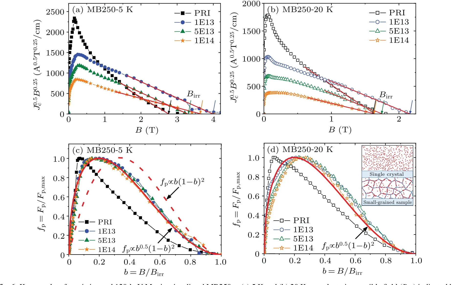
Fig.6.Kramer plots for pristine and 120-keV Mn-ion-irradiated MB250 at(a)5 K and(b)20 K to evaluate irreversible field(Birr)indicated by arrows.Normalized flux pinning force density(fp)with respect to reduced magnetic field(b)at(c)5 K and(d)20 K for pristine and 120-keV Mn-ion-irradiated MB250.The red solid line and the red dashed line represent the fitting curves for surface pinning and normal point pinning,respectively.Inset of Fig.5(d)illustrates the schematic view of the distribution of irradiation-induced defects in single crystals and the films with small grains.
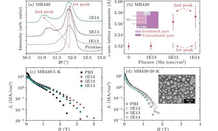
Fig.7.(a) XRD patterns of MB430 around the (0002) peak of MgB2.(b) Variation of c-axis lattice constant of MB430 with fluence.(c)-(d)Magnetic field dependence of critical current density(Jc)at(c)5 K and(d)20 K for 430-nm-thick MgB2 films(MB430)before and after 120-keV Mn-ion irradiation.The inset in(d)is the top SEM view for MB430 with an average grain diameter of approximately 140 nm.
The Kramer plots for MB430 at 5 K and 20 K are shown in Figs.8(a)and 8(b),respectively,and theBirrfor each sample was indicated by arrows.Figures 8(c) and 8(d) show normalized flux pinning force as a function of the reduced magnetic field for MB430 at 5 K and 20 K,respectively.Thefp(b)at high fields forb>0.2 and at 5 K overlapped accurately with surface pinning.Although thefp(b)curve exhibits a slight deviation at 20 K,the flux pinning by GBs is still effective even when the thickness of MgB2films is relatively larger than that of the irradiated layertD.These results further support the improvement of the flux pinning effect by GBs in MgB2thin films after irradiation.The sharp peak in thefp(b)curve at low fields was almost suppressed in the irradiated MB250,as shown in Fig.6,indicating that the residual sharp peak offp(b)at low fields in the irradiated MB430 is associated with the unirradiated region.Our findings can provide useful information for designing radiation resistant MgB2because grain boundaries in metallic MgB2superconductors can be acted as an effective sink of irradiation-induced defects,thus irradiation tolerance of MgB2can be enhanced by decreasing grain size.
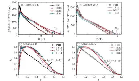
Fig.8.Kramer plots for pristine and 120-keV Mn-ion-irradiated MB430 at (a) 5 K and (b) 20 K.Here, Birr is indicated by arrows.Scaling behavior of the flux pinning force for MB430 at(c)5 K and(d)20 K indicates that the effect of surface pinning is enhanced significantly after ion irradiation.
4.Conclusions
In summary, we observed that the pinning effect by GBs in MgB2thin films can be improved by ion irradiation.The MgB2thin films with nanoscale grains of approximately 122 nm and 140 nm were irradiated with 120-keV Mn ions leading to a significant increase in the field performance ofJcfor all films as compared with that ofJcfor pristine films.Although the GBs of pristine films were not effective for flux pinning,the scaling behavior of the flux pinning force showed that the surface pinning,i.e.,grain boundary pinning,became dominant after ion irradiation.These findings underpin that MgB2superconductors with small grains can be a good candidate for application in irradiation environments,such as nuclear fusion reactor.
Acknowledgements
We wish to acknowledge the support of the accelerator group and operators of KOMAC (KAERI (C.K., J.S.)).Project supported by the National Research Foundation(NRF)of Korea through a grant funded by the Korean Ministry of Science and ICT (Grant No.2021R1A2C2010925 (T.P., Y.H., J.S.)); the Basic Science Research Program through the NRF of Korea funded by the Ministry of Education (Grant Nos.NRF-2019R1F1A1055284(J.M.L.,W.N.K.)and NRF-2021R1I1A1A01043885 (S.G.J., Y.H.)), the National Natural Science Foundation of China (Grant Nos.12035019 (J.L.)).Moreover,L.L.would like to acknowledge the Chinese Scholarship Council(CSC)for fellowship support.
猜你喜欢
杂志排行

Chinese Physics B的其它文章
- Diamond growth in a high temperature and high pressure Fe-Ni-C-Si system: Effect of synthesis pressure
- Multi-channel generation of vortex beams with controllable polarization states and orbital angular momentum
- Calibration of quantitative rescattering model for simulating vortex high-order harmonic generation driven by Laguerre-Gaussian beam with nonzero orbital angular momentum
- Materials and device engineering to achieve high-performance quantum dots light emitting diodes for display applications
- From breather solutions to lump solutions:A construction method for the Zakharov equation
- Complete population transfer between next-adjacent energy levels of a transmon qudit