Atomic-scale electromagnetic theory bridging optics in microscopic world and macroscopic world
2023-11-02ZhiYuanLi李志远andJianFengChen陈剑锋
Zhi-Yuan Li(李志远) and Jian-Feng Chen(陈剑锋)
School of Physics and Optoelectronics,South China University of Technology,Guangzhou 510641,China
Keywords: atomic-scale electromagnetic theory,two-dimensional materials,transfer matrix method
1.Introduction
Electromagnetism,electrodynamics,and optics deal with radiation, transport, detection, reception, and other relevant processes of electromagnetic waves and light in vacuum, air,water, glass, crystal, cable, fiber, and other media and materials, either transparent or opaque, homogeneous or inhomogeneous, isotropic or anisotropic.In the past centuries, the physics concepts, rules, laws and theories describing electromagnetics have become pretty mature and can be found in many standard textbooks of classical electromagnetism,electrodynamics and optics.[1,2]The bases behind them are Maxwell’s equations describing the evolution of electric and magnetic fields under the actions of electric charges and currents.In the simplest situation of vacuum, Maxwell’s equations are written as follows:
In history,these equations have successfully predicted the existence of electromagnetic waves in a vacuum and inferred that light is a kind of electromagnetic wave.In a vacuum,electromagnetic waves are transverse waves with their electric and magnetic fields oscillating (polarized) in the plane perpendicular to the transport direction.These waves are expressed by mathematical functions asE=E0e-iωt+ikzandH=H0e-iωt+ikz.Here, we have assumed a monochromatic electromagnetic plane wave with an angular frequencyω,wavelengthλ,and wave vectork=ω/c=2π/λ(wherecis the speed of light in a vacuum)transporting along thez-axis direction.The electric and magnetic field amplitudes(E0,H0)are polarized in the transversexoyplane.
In a more complicated situation of an isotropic,homogeneous, nonmagnetic dielectric medium, the popular assumption for a long time is the electromagnetic waves transport in a macroscopically continuous medium described by the constitutive relation of the electromagnetic medium asD=ε0E+P,P=χE,B=µ0H,wherePrepresents the macroscopic polarization of the medium.Then Maxwell’s equations are written as follows:
Here,we only consider an isotropic and nonmagnetic medium where the electric susceptibilityχand dielectric constantεare isotropic scalar quantities.However, more general situations can be handled similarly.These equations form the basis for implementing a complete description of the electromagnetic field evolution and electromagnetic wave transport within a medium, other than the simplest situation of vacuum isP=0,D=ε0E, andB=µ0H.Within a homogeneous and isotropic dielectric medium, electromagnetic waves are still transverse waves,but the electromagnetic fields are now expressed asE=E0e-iωt+iknz,H=H0e-iωt+iknz,wheren=εis the refractive index of the dielectric medium.When combined with electromagnetic boundary conditions for macroscopic media, these equations readily handle reflection, transmission, refraction, and absorption of electromagnetic waves across the interfaces between two media.The corresponding reflection,transmission,and absorption coefficients can be extracted using the well-established Fresnel formula.[1,2]This macroscopic electromagnetic theory can be extended to handle the general problem of wave transport in complicated media composed of a cascade of multiple homogeneous media, possibly with the assistance of analytical and numerical tools like transfer-matrix method.[3-5]The differential Maxwell’s equations can also be solved numerically using complex yet elegant approaches such as the finite-difference time-domain method[6]and the finite-element method,[7]which are available under commercially available software packages.[8,9]These numerical approaches can handle arbitrary complicated inhomogeneous optical media, materials, and devices with micro/nanoscale modulation on the dielectric constant.
One crucial ingredient for the macroscopic electromagnetism,under the macroscopic Maxwell’s equations described in Eq.(2), is the derivation of macroscopic polarizationP.This polarization is an averaged quantity for a sufficiently large volume (ΔV), involving a large number of atoms/molecules(with dipole momentPi,i=1,2,...,N)that comprise the medium,as given by
Obviously, this macroscopic model is accurate in principle only when ΔVis much larger than the size of a single atom/molecule, and the numberNis much larger than 1.Within the framework of this macroscopic model,all electromagnetic phenomena occur within continuous media, except for the interface between two media, where the discrete nature of atom/molecule is completely absent.The electromagnetic properties of the medium are solely described by the phenomenological continuous function ofχandε.In the long history,people have always assumed that this macroscopic electromagnetism model maintains perfect accuracy and poses no problem.
Yet, surfaces and interfaces always exist in any electromagnetic media, and discrete nature of atoms/molecules is expected to manifest in the electromagnetic field and wave around and within these surface/interface atoms/molecules.This leads to some certain discrepancies (with the exact extent of discrepancy unknown) from the predictions and descriptions made by the macroscopic electromagnetic model,especially at the atomic and sub-atomic scale near the surface/interface.Besides, in the past decade, two-dimensional(2D) materials like graphene, MoS2, black phosphorus, heterogeneous van de Waals materials,and many others have attracted great interest in multidisciplinary areas of science and technology.[10-15]For these homogeneous/heterogeneous natural 2D materials,with each composite atomic layer having a thickness(less than or close to 1 nm)several orders of magnitude smaller than the wavelength of light,and with the overall thickness of a regular 2D material sample still far smaller than the wavelength of light,it is naturally expected that the macroscopic electromagnetic model will encounter some inaccuracy problems, although the extent of deficiency is unknown.To address these fundamental questions,it is highly desirable that we transition from the macroscopic electromagnetic model to a more deliberate microscopic electromagnetic model.Such a model can handle the above atomic-scale electromagnetic field and wave issues on the one hand and can evolve to address macroscopic electromagnetic field and wave issues with high accuracy at a size scale comparable and far larger than the light wavelength.
In this paper, we develop and present a systematical atomic-scale electromagnetic theory,aiming to fulfill the fundamental purpose of building a bridge connecting optics,electromagnetics, and electrodynamics in the microscopic and macroscopic worlds.In Section 2, we provide a detailed discussion on constructing such a theory and present the specific procedures by first considering the simplest situation of light normally transporting through a homogeneous medium.We divide the three-dimensional (3D) homogenous medium into a periodic stack of a series of single 2D atomic layers and introduce the atomic volume polarizability and atomic-layer line polarizability as critical physical quantities to describe the optical response of each atom and atomic layer, respectively.Then, we transform the solution of vacuum Maxwell’s equations into the construction of a one-dimensional (1D) single atomic-layer transfer matrix.This matrix serves as the building block of the atomic-scale electromagnetic theory,enabling us to handle all light transport properties,including the transmission/reflection coefficients, effective refractive index, and dielectric constant, for this homogeneous medium.In Section 3,we proceed to handle the more complicated problem of light transport through a homogeneous medium with atomiclayer defects and a general heterogeneous medium composed of multiple chemically different layers.The key to the power of theory lies in directly combining individual single-layer transfer matrices for different 2D material atomic layers and incorporating them into the framework of 1D transfer-matrix method.In Section 4,we address the transport of obliquely incident light through homogeneous and heterogeneous media,with the central point remaining the construct of the single atomic-layer transfer matrix.By separately considering the TE and TM polarizations, we transform the 3D electromagnetic problem into simple problems that can be solved using the 1D transfer-matrix method.In Section 5, we consider an extreme situation where light propagates laterally within the 2D plane of a single or a few atomic layers.We will answer the fundamental question of whether or not light can be confined and localized within a single atomic layer or a few atomic layers with thickness several orders of magnitude smaller than the wavelength of light.
In Section 6, we present a few examples of calculations to demonstrate how to use the methodology of the developed atomic-scale electromagnetic theory to handle light transmission/reflection through a single atomic layer, a homogeneous medium plate consisting of an arbitrary number of layers, a homogeneous medium with atomic-layer defects, and a heterogeneous medium composed of several chemical types of atomic layers.In Section 7, we further discuss several important issues that cannot be completely addressed within the framework of the developed atomic-scale electromagnetic theory.One issue is the determination of the atomic volume polarizability and atomic-layer line polarizability,which can either be calculated in the framework of quantum mechanics or measured via careful and deliberate experiments.The other issue is how to extend the developed atomic-scale electromagnetic theory from optics for simple single-element materials to handle optics for more complicated multiple-element compound materials.Finally, in Section 8, we present a full, deliberate,yet compact summary of this lengthy paper and offer an extensive perspective of the developed atomic-scale electromagnetic theory.This theory serves as a high-efficiency bridge connecting optics, electromagnetics, and electrodynamics in the microscopic and macroscopic worlds, connecting classical optics with quantum mechanics, and extending from 1D atomic-scale optical problems to more complicated 2D and 3D atomic-scale optical problems.
2.Atomic-scale electromagnetic theory for homogeneous-material medium
Let us first consider the simplest model of a macroscopic solid dielectric medium and its microscopic building element,as shown in Fig.1(a),where each particle represents an atom,and each microscopic unit cell contains only a single atom.Thus, along the light propagation direction, the macroscopic solid medium can be looked upon as a periodic stacking of single atomic layers,as seen in Fig.1(b).The critical point of this microscopic electromagnetic theory is then to first explicitly determine the optical response of this single atomic layer in terms of well-known and popularly-used macroscopic optical quantities,such as transmission,reflection,and absorption coefficients for both the optical field and intensity.When this procedure is successful,we are then able to place all these microscopic electromagnetic quantities into the well-established physical framework of macroscopic electromagnetism, electrodynamics,and optics.
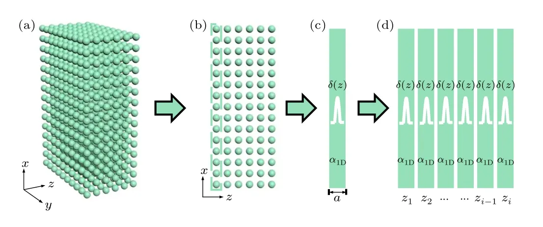
Fig.1.Schematic for the atomic-scale electromagnetic theory bridging optics in the microscopic world and macroscopic world.(a) A macroscopic optical crystalline medium is considered as a three-dimensional stack of its fundamental building block: discrete atoms embedded within vacuum.(b) Along the transport direction of light, the medium can be viewed as a one-dimensional periodic stack of single atomic layers as the building blocks.(c) The optical response of each atomic layer can be modeled as a δ function representing the polarized charge and current induced by the local electric field.(d)The whole medium can be modeled as a periodic stack of multiple δ functions.
2.1.Introduction of atomic polarizability into vacuum Maxwell’s equations
Let us begin the discussion with light transport in a dielectric medium.Traditionally,one would consider the evolution of the electromagnetic field and the motion of electromagnetic wave in a continuous dielectric medium, whose optical response is described entirely and perfectly with permittivity and permeability.However,there is another naive,yet unusual and natural way of thinking: looking upon all dielectric media as composed of a large number of discrete atoms embedded within the vacuum background.In this perspective, each atom is polarized by the electric field of the illuminated external light,and the optical response of each atom is represented by a point dipole with a moment related both to the local electric fieldEi(r)and atomic polarizabilityαi.All these atomic dipoles serve as secondary radiation sources,emitting optical waves, inducing multiple scattering between atomic emitters,and eventually resulting in the stabilized macroscopic optical field evolution and wave transport.
Based on this physical insight and operational methodology,the classical Maxwell’s equations Eq.(2)for light transport in a homogeneous dielectric medium can be reformulated as follows:
Under the popular situation of harmonic wave excitation with time dependent function ofE(r,t)=E(r)e-iωt,H(r,t)=H(r)e-iωt,Eq.(4)becomes
Indeed, Eqs.(4) and (5) indicate a significant departure from the traditional view of electromagnetic field and wave transport within a macroscopic continuum medium.Instead, they suggest that electromagnetic field and wave now transport through a cloud of discrete atoms, which are numerous in amount and situated in vacuum, interacting via fundamental forces of nature.Unlike Eqs.(1), (4) and (5) include electromagnetic radiation sourcesJembedded within the vacuum background.However, the challenge lies in the fact that the radiation sourceJis unknown,as it depends on the yet-to-bedetermined local electric fieldE.Consequently, our current task is to find a solution to these two coupled equations,which represent the microscopic Maxwell’s equations.It is important to note that we have assumed a single-element medium,where all atoms are identical and possess equal atomic polarizability.The precise determination of the radiation sourceJrelies on the solution for the local electric fieldE.Solving these coupled equations represents a crucial step in our effort to develop the atomic-scale electromagnetic theory.
2.2.Solution of microscopic Maxwell’s equations for single atomic layer
In this scenario,we focus on the optical response of a single atomic layer and examine the behavior of light as it travels through this layer.We consider the simplest case where the incident light is normally directed onto the atomic layer and propagates parallel to the stacking direction of atomic layers,represented by thez-axis.The incident light is a transversepolarization electromagnetic wave, with its electric field and magnetic field aligned along the transversexandyaxes, respectively.Let us assume that the electric field is polarized along thex-axis,and the atomic layer is located atz=0.Then,we can express the electric field asE(r)= ˆxE(z)and the magnetic filed asH(r)=ˆyH(z).With this setup, we can simplify the microscopic (or atomic-scale) Maxwell’s equations into the following form:
which can be further simplified into
Notice that the solution procedure remains the same when the electric field is polarized along theyaxis.Reaching the final step of Eq.(7), we consider all atomic dipoles within the atomic layer, with a total number beingN, and calculate the average atomic density as 1/ΔS, assuming the average area occupied by each atomic dipole is ΔS.Consequently, the effective atomic polarizability for this atomic layer is given byα/ΔS.In some sense,αcan be regarded as the volume atomic polarizability, whileα/ΔScorresponds to the atomiclayer line polarizability.Solving Eq.(7)may seem a little unusual in optics.However,upon further consideration and reference, one can make a comparison with the well-known 1Dδ-function problem in quantum mechanics, which provides a clue to the answer.Let us briefly analyze the physics picture.The incident light propagates from left to right and strikes the atomic layer,inducing polarization of atoms and leading to reflection and transmission of light, as commonly observed in optics (as illustrated in Fig.1(c)).The solution of Eq.(7)indicates that the electric field distribution can be written as follows:
Besides, some physical and mathematical reasoning arguments upon Eq.(7)also suggest the following connection conditions atz=0 where the atomic layer sits:
Definingα1D=α/(ΔSε0)as the line polarizability of atomic layers and combining Eq.(8) with Eq.(9), we immediately find
A simple derivation finally gives
Equation (11) provides the explicit formulation of the transmission and reflection coefficients for light passing across a single atomic layer, directly describing the optical response of that atomic layer.It is worth noting that we do not directly adopt the electromagnetic field continuity boundary condition commonly used in classical electrodynamics textbooks.Instead, we mathematically derive the boundary condition Eq.(9)directly from Eq.(7),specifically,we obtain the magnetic field boundary condition(the second part of Eq.(9))by integrating both sides of Eq.(7).The integration operation involving theδ-function leads to a discontinuity of the first derivative of the electric field,which translates to a discontinuity of the magnetic field.In physical terms,the single atomic layer exhibits an infinitesimally-thin polarized current (surface polarization current)excited by the incident electric field.This surface current induces the discontinuity of the magnetic field.It is important to highlight that in classical electromagnetics and electrodynamics, the theory primarily deals with macroscopic dielectric or metallic slabs, not infinitesimallythin atomic layers.Consequently,only free current(not polarization current) will induce the discontinuity of the magnetic field in classical theory.Moreover,at optical frequencies,the electric field does not induce free current,resulting in both the electric and magnetic fields being continuous across a dielectric/metallic slab surface.
2.3.Solution of microscopic Maxwell’s equations for multiple atomic layers
As we progress to handle a slab of medium composed of a stack of a series of atomic layers, we can follow a similar procedure as we did for Eq.(7).Consequently, we find the simplified 1D model to be
Here,Nrepresents the number of atomic layers along the light transport path.To solve this optically coupled system of multiple atomic layers, we adopt the well-established transfermatrix method.[3-5]This method first focuses on constructing the transfer matrix for each individual atomic layer, then employs an iteration algorithm to derive the overall transfer matrix for the system, and finally calculates the transmission and reflection coefficients,as well as the electromagnetic field within the system.It should be noted that Eq.(12) describes the wave transport across multiple atomic layers and is solved using the transfer-matrix method.In this formalism,the electromagnetic interaction/coupling between different layers has been fully incorporated within the individual atomic-layer transfer matrix.The complex amplitudes of the forward incoming wave and its reflection wave,as well as the backward incoming wave and its reflection wave across each individual atomic-layer, are all unknown due to the interaction/coupling between different layers,and they need to be solved.
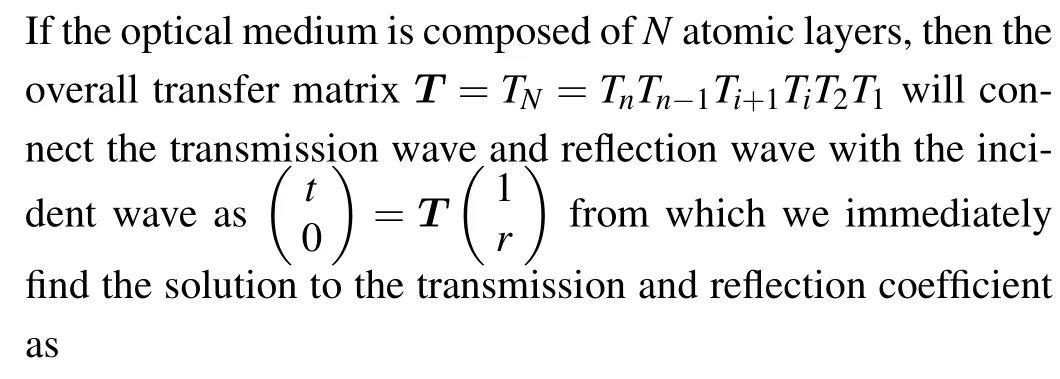
As shown in Fig.2(a),consider thei-th atomic layer,the electric fields at the two sides are written as
Implementing the connection conditions atz=zisimilar to Eq.(11),we find
Assuming the distance between thei-th and(i+1)-th atomic layer isai=a,then we find that the field at the left hand side of (i+1)-th atomic layer is related with the field at the left hand side ofi-th atomic layer via the following unit-cell transfer matrix:
Equations (11), (15), and (16) essentially form the fundamental formulation connecting macroscopic optical quantities,such as the transmission and reflection coefficientstandr,and the wave vector of the light wavek,with the microscopic physical quantities related to atom layers.These include the atomic polarizabilityα,the effective cross-section of an atom within an atomic layer ΔS,the atomic-layer line polarizabilityα1D, and the atomic layer separation size (or lattice constant for crystalline medium)a.Following Eq.(16)and calculating the reflection wave and field,as well as the transmission wave and field, we can continue to use the transfer-matrix method with Eqs.(13)and(15)to calculate the internal wave and field everywhere inside the medium.These equations play a crucial role in bridging the microscopic and macroscopic worlds, allowing us to understand the behavior of light at both atomic and macroscopic scales.
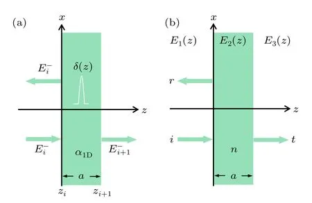
Fig.2.Schematic for the solution of the macroscopic plate under atomic-scale theory and classical-optics theory.(a) Atomic-scale theory.(b)Classical-optics theory.
2.4.Retrieval of characteristic transport feature of light in crystalline medium
In the above, we establish a connection between the macroscopic optical transport properties for a continuous medium slab and the microscopic physical quantities of the composite atoms in response to light.In a sense,the transmission, reflection, and absorption coefficients for both the optical field and energy are all extrinsic quantities that reflect the physical and optical properties of the medium as a whole.However,the more important and desirable goal is to identify some intrinsic physical quantities.
2.4.1.Dispersion relation of light transport
Classical optics states that the transport of light within a continuous medium is characterized by the mere physical quantity of refractive indexnand dielectric constantε(withε=n2), as shown in Fig.2(b).Besides, the intrinsic transfer matrix of an electromagnetic wave traveling within this continuous medium across thei-th layer of a distanceais given by
and its eigenvalues are
Furthermore, we also solve the eigenvalues of single-layer transfer matrix Eq.(15)and get its eigenvalues as
We construct an equationf(ka) = cos(kna)-cos(ka)+(1/2)kα1Dsin(ka), and can obtain the relationship between the microscopic polarizabilityα1Dand the macroscopic refractive indexnby carrying out the Taylor series expansion on this equation.Whenka=2πa/λtends to zero,e.g.,for the current whereλ ≫a,we perform Taylor series expansion onf(ka)atka=0 and can get
2.4.2.Effective dielectric constant and refractive index
When we take the first-,second-and third-order approximations,we can get
The above relations have built the connection between the microscopic polarizability and the macroscopic refractive index.When we consider the first-order approximation, we can obtain the following explicit relationship:
When we consider the second-order approximation, we can get the following explicit relationship:
2.5.Transmission and reflection for homogeneousmedium plate under atomic-scale theory and classicaloptics theory
We proceed to consider light transport through a microscopic or macroscopic homogeneous-medium plate with arbitrary thickness(or atomic layer number)in the framework of both the atomic-scale electromagnetic theory and the more familiar classic optical theory.Suppose a homogeneous plate has a thickness ofdand consists ofNatomic layers, whereNcan be any arbitrary integer number.In the atomic-scale electromagnetic theory, according to Eq.(16), the overallTmatrix is given by
One way to calculate the macroscopic plateT-matrixTis via direct computation of matrix multiplication following Eq.(25).Yet, it is worthwhile to have a deep analysis and further simply the calculation of Eq.(25)by using the characteristic matrix(or eigenvector matrix)of single-layerT-matrixTicorresponding to the eigenvaluesλ3,4.It is easy to find that the corresponding eigenvector is
By defining a matrix as
we find the following formulation:
Then it is easy to find that
Comparison between Eqs.(28) and (29) indicates that the macroscopic plateT-matrix differs from the single-layerTmatrix only in the central phase-transport term.
For comparison, we introduce the calculation method of transmission/reflection coefficients based on the air-medium Fresnel’s formula well known in classical optics.For a plate with a thickness ofdshown in Fig.2,the electric fields of the air and dielectric medium can be represented as
Here the wave vector of light in continuous air and dielectric medium isk1=k0=ω/candk2=nk0.Based on the boundary conditions atz=0 andz=d(d=ja,j=0, 1, 2, 3,...),we can get
where the matrix element is given by
Finally,letA=1,A'=r,C=t,C'=0,the transmission and reflection coefficients of electromagnetic fields are
The energy transmission and reflection coefficients are simplyR=|r|2andT=|t|2respectively.Basically, Eqs.(24)and(30),in combination with Eq.(31),are the formulas used to account for the transmission and reflection coefficients for a microscopic and macroscopic homogeneous plates.Note that when the atom polarizability is anisotropic, we can treat it as a tensor and solve the electromagnetic field distribution based on boundary conditions.This allows us to capture the full polarization response of the single-layer or few-layer twodimensional materials,considering its directional dependence.Besides, it should also be emphasized that not only the conductivity with an imaginary part in the permittivity can be considered,but also the dielectric tensor with dispersion response can be processed.
3.Atomic-scale electromagnetic theory for heterogeneous-material medium
In Section 2, we consider a homogeneous crystalline medium composed of a periodic stack of uniform single atomic layers.The atomic-scale electromagnetic theory developed for this simple yet general problem serves as a bridge between optics in the microscopic and macroscopic worlds.This theory is applicable to the contemporary hot issues in optics,particularly for materials science and the fascinating domain of 2D materials.In this section, we further explore several more complicated scenarios involving atomic layer stacks and buildings.
3.1.Homogeneous medium with atomic-layer defect
As illustrated in Fig.3(a), the first situation we consider is a homogenous medium built from a periodic stack of matrix atomic layers with line polarizabilityα1D,0and layer thicknessa0.Within this medium, there exists a defect atomic layer with line polarizabilityα1D,dand layer thicknessad.This defect atomic layer can either be a vacancy withα1D,d=0,where the original atomic layer is missing for some reason,or be another atomic layer replacing the original one.Notice that such atomic-scale defected media are hard to calculate using the classical continuum-medium optics method,as a single atomic layer cannot be adequately described by the continuum-medium model.However,this problem can be readily handled by the current atomic-scale electromagnetic theory.Moreover, the methodology developed in Subsections 2.2 and 2.3 is based on the single-layer transfer matrix,enabling theoretical calculations for both defected and perfect media to be performed within the same background.Suppose the matrix-medium atomic-layerT-matrix isT0,while the defect atomic-layerT-matrix isTd, and they are respectively given by
For a medium composed ofNmatrix-medium atomic layers,a single defect atomic layer, andMmatrix atomic layers, the overallT-matrix for the defected matrix medium slab is then
With the overallT-matrix at hand, the calculation of transmission wave and field,the reflection wave and field,and the internal wave and field at the matrix-medium atomic layers and the defect atomic layer is straightforward, following the procedures presented in Subsection 2.3.On the other hand,if the matrix medium involves multiple defect atomic layers,either homogeneous-material layer or heterogeneous-material layers, the calculation procedure is also similar.This means that the developed atomic-scale electromagnetic theory has a broad range of applicability.
Fig.3.Homogeneous medium with atomic layer defects and heterogeneous medium composed of a series of different atomic layers stacked one by one.(a) Schematic illustration of homogeneous medium (green regions)with atomic layer defects(gray regions).(b)Schematic illustration of the heterogeneous medium.There are three different atomic layers(blue,orange and green regions)in a period.
3.2.Heterogeneous medium
As shown in Fig.3(b), the second situation we consider is a heterogeneous medium composed of a series of different atomic layers stacked one by one.Suppose the heterogeneous slab hasNatomic layers, and thei-th atomic layer has the atomic polarizabilityα1D,iand layer thicknessai.Then thei-th atomic-layerT-matrixTiis given by
Based on all the individual atomic-layerT-matrix,theN-layer heterogeneous slab has the overallT-matrix given by
In addition, if the heterogeneous slab forms a macroscopic composite medium by stackingMperiodic slabs, then the overall heterogeneous plate has theT-matrix given by
Having obtained theT-matrix for a heterogeneous slab or macroscopic plate,all the optical properties,including the reflection and transmission coefficient,the electromagnetic field within the heterogeneous, and the effective refractive index and dielectric constant for the composite heterogeneous slab,can be derived and calculated.Besides, Eqs.(35) and (36)can also encompass the more general situation where a defective atomic layer exists within the heterogeneous materials and structures.
4.Atomic-scale electromagnetic theory for oblique incidence of light
In Sections 2 and 3,we consider the simplest light propagation situation where the illumination light is normally incident upon a single atomic layer,a multiple atomic-layer slab,and a macroscopic dielectric medium slab.In this simplest configuration, the atomic-scale electromagnetic theory only needs to handle the simplest 1D problem of optics and electromagnetics,which is a scalar-wave transport problem.It turns out that this 1D optical problem can be solved by adopting a procedure similar to the well-established quantum mechanical problem of electronδ-functional potential barrier.Yet, it is necessary to extend this theory and consider a more general configuration where the illumination light is obliquely incident upon a single atomic layer, a multiple atomic-layer slab,and a macroscopic dielectric medium slab.When doing this,we find it is difficult to follow the simple 1D scalar-wave solution procedure as developed in Section 2 to solve these more complicated problems of atomic scale optics and electromagnetics.Rather, we should stand within the framework of classical electrodynamics and solve the transport of vector light and electromagnetic waves across the atomic layer.We have found the critical point in the whole procedure of solution is the construction of the connection/boundary conditions of electromagnetic fields across the atomic layer,and this has been placed in the Appendix with great details.
It is well established in classic optics that the vector wave transport through an optical slab or current atomic layer is basically a 3D problem,but it can be simplified and decomposed into 2D problems with TE and TM polarization with respect to the naturally selected light incidence plane.In the following we present the atomic-scale electromagnetic theory for the general situation of oblique incidence.We will focus on the solution of electromagnetic field for light passing across a single atomic layer,and then the construction of theT-matrix for this atomic layer, since it is clear from Sections 2 and 3 that these two steps are standing on the center core of our atomicscale electromagnetic theory.In the following we will address how this general situation can be handled analytically.
4.1.TE polarization
In this polarization state, the non-zero EM field component is (Ey,Hx,Hz).According to the schematic picture of Fig.4(a), the atomic layer is still modeled as aδpotential barrier to describe its response to the external field.Suppose the incident light has an inclined angleθagainst the surface normal direction of the atomic layer,so that the tangential and normal wave vector components are given bykx=ksinθandkz=kcosθ.Then the electric field across the atomic layer is given by
The magnetic fieldHxandHzcan be written readily using Maxwell’s equations in vacuum.To determine the light transport characteristics (transmission and reflection) through the atomic layer for a given incident waveE+ieikxx+ikz(z-zi), one should utilize some connection formula (or boundary conditions)for electromagnetic fields across the atomic layer.This has been discussed in great detail in the Appendix material.According to Eq.(A32),we have
After some simple algebraic manipulations,we reach the following transfer-matrix formula as the connection/boundary conditions for fields across the atomic layer:
Further considering the transport phase accumulation within a single atomic-layer unit cell, we can construct the following unit-cellT-matrix:
It is easy to find that for normal incidence,Eq.(42)is identical to Eq.(15).This means that for a simple scalar-wave transport problem,the quantum mechanical solution can yield the same result as the atomic-scale electromagnetic solution.
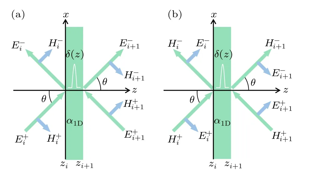
Fig.4.Schematic for solution of light transport through a single atomic layer represented by δ-function polarized charge and surface current in the framework of transfer-matrix method.(a)Oblique incidence situation where TE-polarized light transports with an arbitrary angle with respect to the atomic layer.(b)Oblique incidence situation where TM-polarized light transports with an arbitrary angle with respect to the atomic layer.In these two situations,the incident angle(equal to the transmission angle)is θ,and we have the ordinary 2D optical problems.
4.2.TM polarization
In this polarization state, the non-zero EM field component is (Hy,Ex,Ez).According to the schematic picture of Fig.4(b), the atomic layer is again modeled as aδpotential barrier to describe its response to the external field.Again suppose the incident light has an inclined angleθagainst the surface normal direction of the atomic layer,then the tangential magnetic field across the atomic layer is given by
The other two field componentsExandEzcan be written readily using Maxwell’s equations in vacuum.To determine the light transport characteristic (transmission and reflection) through the atomic layer for a given incident waveone should utilize some connection formula(or boundary conditions)for electromagnetic fields across the atomic layer.This has been discussed in great detail in the Appendix material.According to Eq.(A34),we have
After some simple algebraic manipulation, we have the following transfer-matrix formula as the connection/boundary conditions for fields across the atomic layer:
Further considering the transport phase accumulation within a single atomic-layer unit cell, we can construct the following unit-cellT-matrix:
Now that we have constructed the single atomic-layer unitcellT-matrix,we can follow the similar procedure developed in Sections 2 and 3 to analyze all important characteristics for light propagation through a single atomic layer, multiple atomic layers,and eventually a macroscopic slab composed of a large number of atomic layers,with an arbitrary inclined angle, or an arbitrary value of non-zero transverse wave vector.We can also handle more complicated situations of homogeneous medium embedded with an atomic-layer defect and heterogeneous medium made from a stack of different atomic layers.Extension of the theoretical solution procedure is straightforward and we will not repeat them here.
5.Localized surface state for single and few atomic layers
We continue to consider an interesting question: can a single atomic layer or a thin film consisting of a few atomic layers (either homogenous or heterogeneous) support a localized surface state whose electromagnetic field is confined around the atomic layer or atomic-scale thin film? This is by no means a simple question whose answer is readily known.In the following we will address this fundamental problem by utilizing the methodology developed in Section 4.The schematic illustration of the localized surface state is presented in Fig.5.According to the standard definition in classical optics and electromagnetics, the surface state is a self-sustained eigenmode of an optical system that can exist without an incident light.That is the reason why only outgoing radiation waves are present in Fig.5,and no incoming radiation waves are present.
Let us first consider the TE mode.Equations (38) and(39)now become
The two equations would together yield the non-zero solution of field(i.e.,eigenmode),which exists only when
Then the propagation constant of this localized surface state is given by
We proceed to consider the TM mode.Equations(43)and(44)now become
The two equations would together yield the non-zero solution of field(i.e.,eigenmode),which exists only when
Then the propagation constant of this localized surface state is given by
Obviously Eqs.(50),(51),(54),and(55)tell us that there indeed exists a surface state for both the TM and TE modes even for a single atomic layer.Is this a surprising result that goes a little bit beyond one’s imagination? The answer is yes at least for us before this work.It is also interesting to find that the localization degree of the field,as proportional to|kz|,for the TM mode is much larger than for the TE mode,because
In addition,Eq.(56)indicates that the field at the TE mode is very weakly confined around the atomic layer,while the field at the TM mode is very tightly confined around the atomic layer.
The above theory of localized surface state for a single atomic layer can be extended to examine a more general situation of atomic-scale thin film made from either a few homogeneous atomic layers, or a defective thin film, or a stack of heterogeneous atomic layers.This has to be done by combining the above theory and the methodology developed in Sections 2, 3, and 4.Suppose a given atomic-scale thin film extends in space fromz1andz2,and the correspondingT-matrix connecting the field at the left side and the right side of the thin film isT.Then for the TE mode we have
and for the TM mode we find
Following the definition for the surface state, which does not involve incoming electromagnetic waves,we immediately get the condition of the surface state,which is
for the TE and TM modes, respectively.Equations (59) and(60) yield both the dispersion relation for the localized surface state, namely, the eigenvalue forkx,kzversusk, and the field distribution, namely, the eigenvector for (E+2,E-1) and
(H+2,H-1).
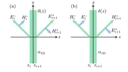
Fig.5.Localized surface states.Illustration of TE-polarized and TMpolarized light.(a)TE polarized light.(b)TM polarized light.
6.Several examples applying the atomic-scale electromagnetic theory
In the above sections,we have presented the atomic-scale electromagnetic theory to solve the transport of electromagnetic waves through a single atomic layer and a thin film composed of general multiple homogeneous/heterogeneous atomic layers under arbitrary incident angles and polarization of light beam by using the microscopic volume and line polarizability to describe the optical response of a single atom and a single atomic layer.To have a clear idea about the power of the atomic-scale electromagnetic theory,here we proceed to show several typical examples.We rigorously solve the transmission spectra of electromagnetic waves in three typical media via the atomic-scale electromagnetic theory, including a homogeneous medium plate with increasing numbers of atomic layer, a homogeneous medium with defects and a heterogeneous medium.Notably,we have built the connection between the microscopic polarizability and the macroscopic refractive index in Section 2.So when the microscopic polarizability cannot be acquired directly, it also can be indirectly obtained according to the relationship between the macroscopic refractive index and the microscopic polarizability,while the macroscopic refractive index usually is easy to be measured experimentally in actual situation.In subsequent calculations,without special notice,we will adopt the explicit relationship under the first-order approximation shown in Eq.(23)to acquire the microscopic polarizabilityα1D=(n2-1)a.
6.1.Homogeneous-medium plate under atomic-scale theory and classical-optics theory
We first calculate the transmission spectra of electromagnetic wave for a microscopic diamond plate composed of various atomic layer numbers under both the atomic-scale theory and the classical-optics theory and make a comparison between the microscopic and macroscopic theories.The macroscopic refractive index of the diamond isn0= 2.417 and the thickness of the single atomic layer of diamond isa0=0.375 nm, so the atomic polarizability of the diamond isα1D,0=4.84a0=1.82 nm.The excitation wavelength of the incident plane wave isλ=1550 nm.
The calculation results are illustrated in Fig.6,where the red solid lines and blue dotted lines represent the results calculated by classical-optics macroscopic theory and atomic-scale microscopic theory,respectively.As shown in Fig.6(a),when the atomic layer numbers are relatively small, e.g., only below 10 layers, the thickness of the plate (3.75 nm) is much smaller than the excitation wavelength of the incident plane wave(λ=1550 nm).In this case,both theories show that the transmissions are almost 100%, but the calculation results of atomic-scale theory(blue dotted line)are slightly smaller than those of classical-optics theory (red solid line) and the transmission differences between them are about 0.03%, a small discrepancy but already remarkable considering the governing position of macroscopic Maxwell’s equations.Moreover,Fig.6(b)shows that as the layer number increases to 100(the thickness of plate is 37.5 nm), the two transmission coefficients calculated by two theories decrease to 0.88 gradually,and their differences are still much smaller than the absolute transmission strengths.
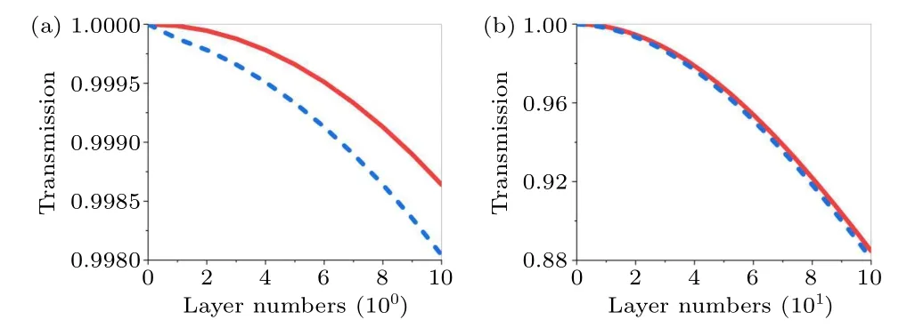
Fig.6.Transmission for macroscopic diamond plate under atomic-scale theory and classical-optics theory.The red solid lines and blue dotted lines are calculated by classical-optics theory and atomic-scale theory respectively.In panels(a)and(b),the transmission spectra of various layer numbers: (a)up to 10 layers and(b)up to 100 layers.The single atomic layer thickness is 0.375 nm,the atomic polarizability is 1.82 nm and the excitation wavelength is 1550 nm.
6.2.Homogeneous medium with atomic layer defects
We continue to calculate the transmission spectra of electromagnetic wave in the homogeneous medium with atomic layer defects by using the atomic-scale theory.Figure 7(a)shows the schematic illustration of homogeneous medium composed of stacked graphene atomic layers (green regions)with atomic layer defects (gray regions).The macroscopic refractive index of graphene at an excitation wavelength ofλ=1550 nm isn0=1.59+1.21i and the thickness of single graphene atomic layer isa0=0.360 nm,so the atomic line polarizability of graphene isα1D,0=0.023+1.385i nm.Besides,the defect atomic layers are the vacancy withα1D,d=0,and the thickness of single defect layer isad=0.360 nm.Figures 7(b)and 7(c)indicate the transmission spectra of homogeneous stacked graphene medium without and with atomic layer defects of various layer numbers.The red solid lines and blue dotted lines represent the transmission curves without and with atomic layer defects respectively.On the one hand, one can see that, for the homogeneous graphene medium without any defects, the transmission strengths (red solid curves) decrease gradually with the increase of atomic layer due to the existence of nonzero imaginary atomic polarizability.On the other hand,for the homogeneous medium of 10(or 100)layers with 2(or 20)atomic layer defects plotted in Figs.7(b)and 7(c),where the atomic layers extend from 5th to 6th layer,and from 41th to 60th layer,respectively,are defects(gray region).By making a comparison of these transmission spectra,we can see that the existence of defect layers significantly affects the transmission efficiency.On the other hand, the influence of defect layers on the transmissions decreases with the increase of thickness of plate.
6.3.Heterogeneous medium composed of different atomic layers
We proceed to calculate the transport behaviors of electromagnetic wave in a heterogeneous medium composed of a series of different atomic layers stacked one by one, as illustrated in Fig.8.There are four types of atomic layers in a period.The atomic thicknesses of them area1=0.3 nm (blue),a2=0.2 nm (orange),a3=0.4 nm (green),anda4= 0.5 nm (yellow), and their atomic polarizabilities areα1D,1=1.023 nm,α1D,2=0.312 nm,α1D,3=0.896 nm,andα1D,4=2.145 nm.The excitation wavelength of incident plane wave is stillλ=1550 nm.Notably, these thicknesses and atomic polarizabilities are optional and do not correspond to any actual materials here.According to the connection between the microscopic polarizability and the macroscopic refractive index shown in Eq.(23), i.e.,we also can obtain their macroscopic refractive indexes aren1=2.1,n2=1.6,n3=1.8, andn4=2.3, respectively.The transmission spectra of heterogeneous medium with various layer numbers are calculated, such as 100 layers in Fig.8(b)and 1000 layers in Fig.8(c).When the plate is 100 layers,the transmission strength is about 0.963,as seen in Fig.8(b).Besides, when the thickness increases to 1000 layers, the transmission strength decreases and then increases.Especially,when the atomic layer is 500,the transmission strength reaches the minimum value of about 0.73,as shown in Fig.8(c).
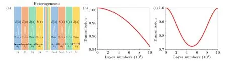
Fig.8.Heterogeneous medium is composed of a series of different atomic layers stacked one by one.(a) Schematic illustration of the heterogeneous medium.There are four different atomic layers in a period.The atomic thicknesses of them are a1 =0.3 nm (blue), a2 =0.2 nm(orange),a3=0.4 nm(green),and a4=0.5 nm(yellow),respectively,and their atomic polarizabilities are α1D,1=1.023 nm,α1D,2=0.312 nm,α1D,3=0.896 nm,and α1D,4=2.145 nm,respectively.(b)and(c)The transmission spectra of heterogeneous medium of various layer numbers:(b)100 layers and(c)1000 layers.The excitation wavelength is 1550 nm.
7.Further discussions
7.1.Accounting for atomic polarizability
In the above atomic-scale electromagnetic theory,we find that the atomic polarizability (either single-atom volume polarizabilityαor single atomic-layer line polarizabilityα1D)stands right at the center core.Consequently,the precise value of these two physical quantities is pivotal for quantitative understanding and prediction of various optical characteristics.In the above sections, we have adopted a simplified model whereα1Dis assumed to be a constant quantity for any homogeneous medium made from uniform atoms and atomic layers, irrespective of the number of atomic layers comprising the concerned microscopic/macroscopic slab.From general knowledge of condensed matter physics,this simplified model means that when the slab increases its thickness layer by layer,the optical response of each layerα1D,ikeeps unchanged and maintains the value of an individual isolated atomic layerα01D.Obviously this is an approximation and has neglected the modification upon the single atomic-layer optical response from other atomic layers due to mutual interaction (atomic-scale microscopic electronic and chemical interactions)between adjacent layers (nearest neighboring, second-nearest neighboring, etc.).Of course, this approximation could be very accurate for some materials with weak layer-to-layer electronic and chemical interactions and couplings,such as conventional graphite(made from periodic loosely stacking of single-layer graphene) or contemporary van der Waals materials (made from arbitrary loosely stacking of heterogeneous single-layer 2D materials).
It is well-known in classical optics and electromagnetics that one can solve Maxwell’s equations and calculate the above relevant optical quantities only when the dielectric constant and refractive index distribution functionε(z) andn(z)are known a priori.Without the knowledge ofε(z) andn(z),optics and electromagnetics would completely fail to describe and predict all optical and electromagnetic phenomena in the macroscopic scale.The situation is similar in the current realm of microscopic optics and electromagnetics.Now in our atomic-scale electromagnetic theory, the atomic polarizabilityα1D,iplays the same role asε(z) andn(z) in the classical macroscopic optics and electromagnetics.Without the knowledge ofα1D,i, the microscopic optics and electromagnetic would also fail to describe and predict all optical and electromagnetic phenomena on the microscopic scale.
In the classical optics and electromagnetics, one usually adopts some well-established and highly accurate experimental approaches and techniques to determine the value ofεandnfor a homogeneous medium and material.For instance,the powerful methodology of ellipsometer measures the amplitude and phase of reflection light for an incident plane-wave light against the surface of a homogeneous medium sample,and then extracts the value ofεandnbased on the Fresnel formula well-known in classical optics and electromagnetics.This standard approach applies to numerous materials and media,either dielectric or metallic materials,either solid or liquid media.These data have been summarized in many handbooks and databases of optical constants, allowing for easy search,access,and are used by general readers and users.
On the other hand, one can also adopt some theoretical and numerical approaches to calculate the value ofεandn.For example,some of these approaches are based on the quantum theory of solid materials,[18,19]where one first calculates the microscopic electronic structures, examines the linear optical response against eternal light, extracts the macroscopic permittivityχ,and finally determines the value ofεandn.Fairly speaking, these theoretical calculations and numerical simulations are very complicated and troublesome,but usually the accuracy and precision are not satisfactory for many materials compared with experimental data, indicating the inadequacy of contemporary condensed matter theory and methodology in application to handle the optical properties of complex solid and liquid materials.
The situations might be different for single atomic-layer or few atomic-layer 2D materials, where the chemical structures and electronic structures are relatively simpler than 3D solid materials and liquid materials.For van der Waals stack 2D materials,the situations are even simpler,because the interlayer stack is loose and the electronic and chemical interactions are weak, so that the optical responseα1D,iof each atomic layer within the whole van der Waals 2D materials maintain their original value.Since all values ofα1D,iare available, we can adapt the formulation of Eqs.(35)and(36)to account for the overall optical response of this special heterogeneous 2D materials structure.
7.2.From single-element materials to multiple-element compound materials
In the above sections we have considered a simple situation where the unit cell (repeating building block) of solid crystalline material consists of a single atom A, whose optical response is described by the atomic polarizabilityα.Then the crystalline material can be looked upon as the periodic stack of single atomic layer AL, whose optical response can be described by the atomic-layer line polarizabilityα1D=α/(ΔSε0), where ΔSis the average cross-sectional area of the atom along the periodic stacking direction.As we have seen clearly in the above sections,α1Dis the primary microscopic optical quantity that can determine the macroscopic optical quantities,such as the transmission,reflection,absorption,dielectric constant,and refractive index.
In nature, most matters and materials are not made from single-element atoms, but from multiple-elements and multiple atoms within a unit cell,in other words,they are compound matters and materials.How to handle the microscopic optics for such a more complicated situation? The answer still lies at the heart of the above discussions.The compound crystalline solid materials can still be looked upon as a periodic stack of single layer of multiple-atom (noted as A1, A2, and so on),which consist of multiple atoms and multiple elements.The critical quantity for microscopic optics is still the line polarizability for the single multiple-atom layer,which is now given by
which assumes that the unit cell consists ofi= 1,2,...,Matoms, each with atomic polarizabilityαiand cross-sectional area ΔSi,respectively.The model of Eq.(61)has decomposed the optical response of the unit cell building the atomic layer and the whole crystalline material.There might be an alternative model where one looks upon the optical response of the unit cell as a whole with an overall volume polarizabilityαcelland effective cross-sectional area ΔScell.Then the single-layer line polarizability is given by
In principle we can perform quantum mechanical simulations to determine the valuesαifor each atom within the unit cell,but the accuracy might not be satisfactory for many complicated compound solid materials.With the single-layer line polarizabilityα1Dand the atomic-layer thickness(also the interlayer distance)aat hand,we can adopt the same formulations as developed in Sections 3,4 and 5 to account for the optical response of a single-layer compound 2D material, multiplelayer homogeneous or heterogeneous compound 2D materials,and eventually the macroscopic crystalline solid compound materials.
A more complicated while also more practical situation is that the compound materials have a large unit cell consisting of multiple atoms in both the lateral cross section and the parallel crystalline axis with respect to the light propagation direction, namely, the 3D unit cell (or repeating cell)involves several atomic layers AL1, AL2, and so on.Then each single multiple-atom layer has line polarizabilityα1D,j(j=1,2,...,N)and layer thicknessaj(j=1,2,...,N),whereNis the layer number within a unit cell along the parallel crystalline direction.α1D,jcan be accounted for by adopting the rule set by Eq.(61) or Eq.(62).With these unit cell optical response quantities at hand, we can adopt the similar formulations as particularly developed in Subsection 3.2 for heterogeneous medium and Subsection 2.3 for periodic atomiclayer stack structure to account for the optical response of these multiple-atom multiple-layer compound 2D materials,thin film,and eventually macroscopic medium.
All the above rules, although complicated and troublesome, can become the basis for building the connection between optics in the microscopic world and the macroscopic world for complex compound matters and materials.It is possible to retrieve the optical response of atoms within each microscopic unit cell from numerous optical measurement data accumulated for so many compound materials existing in nature in the past several centuries.
8.Summary and perspective
We have made a great effort to construct an atomic-scale microscopic electromagnetic theory based on three fundamental aspects of thinking.Firstly,atoms in the microscopic world are the basic building blocks of all matters and materials in the macroscopic world.Secondly,all atoms can be assumed to be sitting and embedded within the vacuum background.Thirdly,optics for macroscopic materials must have a close connection with optics for microscopic atoms.Our prominent goal,seemingly a magnificent dream,is for this atomic-scale electromagnetic theory to become a theoretical system that bridges optics in the microscopic and macroscopic worlds.If this dream comes true, it would represent a significant step towards advancing the fundamental physics of electromagnetics, optics,and electrodynamics to a new horizon and arena.As very few efforts have been made by the optics and electromagnetics community in the past decades,[20]there are very few lessons that can teach and guide us on how to go forward.
To bring such a magnificent dream into reality, we first analyze it in detail and determine the direction to proceed with such a theory.We realize that we must depend on existing theories of prestigious credits instead of creating new ones without significant credit.The choices for the existing theories as a basis for our theory are Maxwell’s equations for the macroscopic world and quantum mechanics for the microscopic world.Following this logic, we find that the electromagnetic and optical wave transport in macroscopic media and materials, which are governed and described solely by Maxwell’s equations,should be closely related to the electromagnetic and optical response of microscopic atoms,which are governed and described by Schr¨odinger’s equation.In this regard, in a qualitative sense, the new theory under construction has already possessed the power to connect microscopic world with macroscopic world and to connect classic physics with quantum physics.
To place the new theory on a quantitatively solid ground,the first step we take is to find and settle down the building block of the theory, which is the microscopic volume polarizabilityαused to describe the optical response of a single atom.This parameter can be used to calculate quantum mechanically by adopting some mature first-principle condensedmatter physics methodologies.The second step is to account for the overall optical response for a single atomic layer consisting of an infinite number of atoms within the cross section perpendicular to the light transport direction.It turns out that the microscopic atomic-layer line polarizabilityα1D,connected with atomic volume polarizabilityαand the effective cross section ΔSvia the formulaα1D=α/(ε0ΔS), can serve as such a critical optical quantity.Based on the quantitative parameter of the microscopic atomic and atomic-layer response,the third step is to account for the macroscopic optical response for such a single atomic layer.To do this we use the only available physics theory for light and electromagnetic wave,i.e.,Maxwell’s equations in the vacuum background,to solve the transport of electromagnetic wave through a single atomic layer under the simplest situation of normal incidence and lateral polarization of plane-wave light, and more complicated situations of arbitrary incident angles and polarization states of plane-wave light beam.With the assistance of well-established 1D transfer-matrix method,we can construct the single atomic layer transfer matrix.We have found that such a microscopic transport quantity holds the key to solving and extracting light transport characteristics for not only single atomic-layer 2D material and few atomic-layers 2D materials, but also many atomic-layers films and macroscopic optical films.With such deep physical insight,the fourth step in our theory is to employ the single atomic-layer transfer matrix,incorporate some simple transfer-matrix methodology,and derive the analytical formulations for all relevant optical quantities.These include the transmission/reflection/absorption coefficient, which are extrinsic optical properties, for different microscopic and macroscopic materials and media, and the dispersion relation, refractive index, and dielectric constant,which are obviously intrinsic optical properties, for macroscopic homogeneous media.In some sense, these four-step procedures comprise the center core of the atomic-scale electromagnetic theory we aim to develop and construct.By making a comparison with solutions obtained based on macroscopic continuum-medium Maxwell’s equations,we can build a bridge between the microscopic atomic polarizability and macroscopic dielectric constant/refractive index.The idea is that when the atomic layer number is very huge, the optics obtained by the atomic-scale electromagnetic theory should accord perfectly with the macroscopic electromagnetic theory based on continuum-medium Maxwell’s equations.
Notice that in the above four-step methodology of atomicscale electromagnetic theory, there is a basic assumption that all atoms and atomic layers are immerged within vacuum, a common background of matter.This is of course consistence with the building law of our world and nature.Such an operation can bring great convenience in the usage of the mathematics of transfer-matrix method and great flexibility in the application of the physical theory, as one can freely incorporate arbitrary building blocks of single atomic-layer transfer matrix(one specific matrix for one kind of atomic layer),into whatever complicated structures and materials by simple operations of permutation and combination,similar to the situation in macroscopic optics.[3-5]As a consequence, the developed theory can handle single-layer and few-layers homogeneous and heterogeneous 2D materials,investigate homogeneous 2D materials with various vacancy or insertion atomic-layer defect,study compound 2D materials with a unit cell composed of several elements in both the lateral and parallel directions with respect to the light transport.Of course, the developed theory can equally handle a macroscopic single-element and compound medium consisting of a large number of homogeneous and heterogeneous atomic layers.Obviously one can see that the new theory can cover a very broad range of microscopic optical problems.
An obvious new power of this atomic-scale electromagnetics theory is that it readily allows one to handle light transmission through single-layer and few-layer homogeneous and heterogeneous 2D materials with/without atomic-layer defects.This power is highly expected and desired by researchers in the material sciences, the big family of 2D materials.Besides, it enables one to examine and answer a fundamental question as to whether or not there exists surface optical states whose electromagnetic fields are confined around a microscopic single atomic layer,although whose size is three orders of magnitude smaller than the wavelength of light.Notice that all these matters are far from continuum medium,and the ordinary dielectric constant and refractive index are not a good quantity to describe optics and electromagnetics,or even hard to define.Therefore in principle,macroscopic Maxwell’s equations, which so far are the only physics theory governing and describing all optical and electromagnetic phenomena,cannot directly apply to these microscopic matters and materials.In this regard, the atomic-scale electromagnetic theory would fill in these big gaps and vacancies of optics and electromagnetics in the microscopic world.
All the new powers promised by the developed atomicscale electromagnetic theory have been well demonstrated by a series of calculation results performed upon several typical examples.This microscopic electromagnetics and optics theory can greatly help to deeply understand all microscopic and macroscopic electromagnetic and optical phenomena from the fundamental atomic origin.More importantly this atomicscale electromagnetic theory can set an example for constructing a bridge of optics, physics and science between microscopic and macroscopic world.Nonetheless, it is worthwhile to notice with caution that the atomic-scale electromagnetic theory alone itself is not able to describe optics and electromagnetics even armed with all the above mentioned promising ways, because it still requires the input of phenomenological microscopic optical response quantities as atomic volume polarizabilityαand atomic-layer line polarizabilityα1D.Ifαandα1Dare unknown, the atomic-scale electromagnetic theory would lose its power.This is similar to the situation of macroscopic optics and electromagnetics,where Maxwell’s equations would lose the power to describe and predict optical and electromagnetic phenomena if the dielectric constantεand refractive indexnare unknown.Therefore,the atomicscale electromagnetic theory should closely work with other physical and chemical theories based on quantum mechanics to find out the atomic and atomic-layer optical responseαandα1Dunder various situations where the electronic/chemical interaction between different atomic layers (adjacent or nonadjacent layers) is weak (thus negligible) or strong (thus not negligible).A more promising way is to work with experimental measurements of macroscopic optical quantities as transmission,reflection,absorption,phase change,and polarization change as a function of light wavelength or frequency, to determine all the microscopic optical response quantities for various matters and materials,either single element or compound,much as macroscopic optics and electromagnetics have done in the past decades and centuries.
Another important issue that we need to take into full account is to extend the current methodology of atomic-scale electromagnetic theory from 1D configuration that applies well to the big family of 2D materials,classical thin film materials,and of course classical homogeneous media,where analytical formulations are available,to more complicated 2D and 3D configurations for the optics and electromagnetics of microscopic wires, fibers, and islands with atomic and nanometer scale far smaller than the wavelength light.Currently the analytical solution and formulation are still not available for 2D and 3D configurations when combined with the point configuration of single atom, and this surely will hinder the construction of simple atomic-scale electromagnetic theory for 2D and 3D and then see what the difference from classical macroscopic electromagnetic theory based on continuum-medium Maxwell’s equations.Yet, the physics and mathematics insight accumulated from the current 1D theory might be a good hint for 2D and 3D theory.Only at that time when all ingredients and methodologies involved within the atomic-scale electromagnetic theory are fully at hand,can the new microscopic theory shine all its great powers in the history of science and technology.
Appendix A: Electromagnetic field radiated by surface currents
(1) Principle of radiation from a single atomic layer modeled asδ-function surface current In this Appendix material, we derive the electromagnetic field radiation from a surface current formed at a single atomic layer and build the boundary condition connecting the electromagnetic field across the atomic layer.The schematic illustration of this problem is depicted in Fig.A1.
We start with the following well-established Maxwell’s equations:
whereJis the polarization current density,and its expression is
The relationship between the vector potentialAand the polarization current densityJis
For the dipole polarization, the electric polarization intensity and the dipole moment satisfy
Combining Eqs.(A2)-(A4),we get
Converted to polar coordinates to solve the double integral,Eq.(A6)can be simplified as
Through the substitution method,the integral part of Eq.(A7)is simplified to
whereJ0(x)is the 0-order Bessel function,i.e.,
(2)Radiation fields of homogeneous wave We first examine the situation where the surface current creates the radiation field of homogeneous wave well studied in classical optics.Whenk >kx,Eq.(A8)is equal to
According to the integral result of Eq.(A8),the vector potential can be obtained as
In the right half plane,z >0,so the magnetic induction intensity can be obtained as
In the left half plane,z <0,we can get the magnetic induction intensity,i.e.,
(2.1)Case of TM mode On the one hand,we consider the TM mode,in this case,the polarization direction is parallel to the incident surface,i.e.,p0=(p0x,0,0),so we get
Thus,the boundary conditions are
which can be written as another equivalent form as
where we have used the connection between the local fieldEand the dipole strengthpthrough the atomic-layer line polarizabilityα1D.
(2.2) Case of TE mode On the other hand, we consider the TE mode,in this case,the polarization direction is perpendicular to the incident surface, i.e.,p0=(0,p0y,0), we can get
Thus,the boundary conditions are
which can also be written as another equivalent form as
(3) Radiation fields of evanescent waves We consider another situation where the surface current creates the radiation field of an evanescent wave,which is also well studied in classical optics.Whenk <kx,the localized surface mode will be excited.Similarly,Eq.(A8)can be changed to
In the right half plane,z >0,the magnetic induction intensity is
In the left half plane,z<0,the magnetic induction intensity is
(3.1)Case of TM mode
On the one hand,we consider the TM mode,in this case,the polarization direction is parallel to the incident surface,i.e.,p=(p0x,0,0),we can get
Thus,the boundary conditions are still
or equivalently
Obviously they are the same as for the homogeneous wave radiation when comparing with Eqs.(A16)and(A17).
(3.2) Case of TE mode On the other hand, we consider the TE mode, in this case, the polarization direction is perpendicular to the incident surface,i.e.,p=(0,p0y,0),we can get
Thus,the boundary conditions are found to be
or equivalently
(4)Extension to general situation of polarization states and radiation angle The above discussions have clearly shown the explicit analytical form of electromagnetic fieldsE,B,andHradiate from a surface current sheet of infinitely thin thicknessJ.More importantly, if this surface currentJis ignited by the incident electric fieldEupon a single atomic layer of line polarizabilityα1D,then the radiated electromagnetic fieldEandHin the left and right hand sides of the atomic-layer surface current have a simple connection formulation.This connection form can set the boundary condition pivotal for solving current problem of light transporting through single and multiple atomic layers.It is well known that in classical optics and electromagnetics for light and electromagnetic wave passing across the boundary of two different dielectric media, the solution of electromagnetic fields based on Maxwell’s equations in each medium and building their connection at the boundary via invoking the well-established boundary conditions (the tangential components of electric and magnetic field must be continuous across the boundary)are two indispensable steps.The boundary condition matching must use the continuous medium permittivityεand permeabilityµ.Now for the current problem of atomic-scale optics and electromagnetics where the continuous medium permittivityεand permeabilityµare no longer applicable accurately, we still can construct the boundary conditions of electromagnetic wave and field when light passes across a single atomic layer, no matter the incident and radiation wave and field are homogeneous or evanescent.For TE mode,the connection/boundary conditions are
or equivalently
While for TM mode,the connection/boundary conditions are
or equivalently
These two sets of connection/boundary conditions,in particular, Eqs.(A32) and (A34) will be used in the entire scope of the current work.
We might consider a more general situation of incident light polarization and inclined angle and construct the connection/boundary conditions of electromagnetic field across the atomic layer.The answer can be found by referring to Eqs.(A31)-(A34),which are
In a more compact form similar to the classical optics and electromagnetics,we have
Herenis the surface normal unit vector of atomic layer, and all the electromagnetic field components take the value right at the site of atomic layer.
Acknowledgments
Project supported by the Guangdong Innovative and Entrepreneurial Research Team Program (Grant No.2016ZT06C594), the Science and Technology Project of Guangdong Province of China(Grant No.2020B010190001),the National Key R&D Program of China (Grant No.2018YFA0306200), and the National Natural Science Foundation of China(Grant No.11974119).
猜你喜欢
杂志排行

Chinese Physics B的其它文章
- Single-qubit quantum classifier based on gradient-free optimization algorithm
- Mode dynamics of Bose-Einstein condensates in a single-well potential
- A quantum algorithm for Toeplitz matrix-vector multiplication
- Non-Gaussian approach: Withstanding loss and noise of multi-scattering underwater channel for continuous-variable quantum teleportation
- Trajectory equation of a lump before and after collision with other waves for generalized Hirota-Satsuma-Ito equation
- Detection of healthy and pathological heartbeat dynamics in ECG signals using multivariate recurrence networks with multiple scale factors