Analysis of displacement damage effects on the charge-coupled device induced by neutrons at Back-n in the China Spallation Neutron Source
2023-09-05YuanYuanXue薛院院ZuJunWang王祖军WeiChen陈伟XiaoQiangGuo郭晓强ZhiBinYao姚志斌BaoPingHe何宝平XuNie聂栩ShankunLai赖善坤GangHuang黄港JiangKunSheng盛江坤WuYingMa马武英andShiLongGou缑石龙
Yuan-Yuan Xue(薛院院), Zu-Jun Wang(王祖军), Wei Chen(陈伟), Xiao-Qiang Guo(郭晓强),Zhi-Bin Yao(姚志斌), Bao-Ping He(何宝平), Xu Nie(聂栩), Shankun Lai(赖善坤),Gang Huang(黄港), Jiang-Kun Sheng(盛江坤), Wu-Ying Ma(马武英), and Shi-Long Gou(缑石龙)
1State Key Laboratory of Artificial Microstructure and Mesoscopic Physics School of Physics,Peking University,Beijing 100871,China
2State Key Laboratory of Intense Pulsed Irradiation Simulation and Effect,Northwest Institute of Nuclear Technology,Xi’an 710024,China
3School of Materials Science and Engineering,Xiangtan University,Xiangtan 411105,China
Keywords: displacement damage effects, charge-coupled device (CCD), China Spallation Neutron Source(CSNS),mechanisms,technology computer-aided design(TCAD)
1.Introduction
The China Spallation Neutron Source (CSNS) is a scientific facility that can provide a wide energy band of pulsed neutrons.[1–3]The back-streaming white neutron source(Back-n)has been exploited as a white neutron beamline which has a wide neutron energy spectrum from eV to hundreds of MeV.It can be used for nuclear data measurement,neutron resonance radiography and analysis of radiation damage.[4–7]
Charge-coupled devices(CCDs)are widely used in many space environments,such as star tracking,space remote sensing and space object detection.However, when used in these applications they can be seriously damaged by particles or rays, leading to degradation of image quality or even functional failure.[8,9]Displacement damage is one of the most important radiation damage effects to a CCD and can be produced by protons,electrons and heavy ions in space radiation environments.Reactor neutrons are often used to analyze displacement damage effects.[10]However, there are also some inconveniences when irradiation experiments are carried out at a neutron reactor.For example, it is difficult to change the beam spot, it takes several days for the neutron activation effects to die down before the irradiated devices can be measured and online radiation effects measurement is complex.The Back-n in the CSNS may solve these problems.Although many studies have already been dedicated to the effects of irradiation on CCDs,[11,12]nearly all the experiments were carried out offline.The process of generating the displacement damage induced by neutrons needs to be investigated by online experiments.The displacement damage mechanism and sensitive volume of the CCD should also be investigated.
This work aims to investigate displacement damage effects on a CCD induced by neutrons at Back-n in the CSNS by an online irradiation experiment.The radiation-sensitive parameters, such as hot pixels, the random telegraph signal(RTS), the mean dark signal and dark signal non-uniformity(DSNU) are measured before and after neutron irradiation.The single-particle displacement damage and transient response are also observed based on the online measurement data.The RTS of the different pixels irradiated by neutrons is investigated.The dark current is calculated according to the mean dark signal at various integration times.The DSNU versus integration time at different irradiation fluences is presented.To analyze the mechanisms of the effects of neutron displacement damage on the CCD,technology computeraided design (TCAD) simulations are performed.This work will provide the basis for theories and experimental techniques for radiation hardening and radiation damage evaluation studies of CCDs.It also provides information for theories and databases to compare the displacement damage effects produced by the reactor neutrons and Back-n.
This paper starts by presenting the main features of the tested device and irradiation conditions.Then, the degradation trends of the hot pixels,dark signal,DSNU and RTS after neutron irradiation are presented.Furthermore, TCAD simulations are performed to analyze the mechanism of neutron displacement damage effects on the CCD.
2.Experimental details
The CCD is irradiated by Back-n in the CSNS.The CCD image array consists of 648×488 pixels and the pixel size is 7.4 µm×7.4 µm.The parameters are measured by a CCD camera.The neutron flux at the exposure position is about 1.4×10⁶neutrons·cm−2·s−1.The neutron energy ranges from eV to∼200 MeV.The accuracy of the fluence and the neutron beam homogeneity is within±10%.A schematic diagram of the experiment is presented in Fig.1.Neutrons incident vertically upon the surface of the CCD array are presented in Fig.2.Air conditioners were used to control the temperature in the laboratory (about 25◦C).The CCD camera was fixed on the worktable.Vertical movement of the worktable can lead to the CCD being irradiated or not irradiated by neutrons.The camera and worktable were controlled by a computer outside the laboratory through network lines.A temperature sensor was inserted into the CCD,and the temperature could be obtained from the camera control system under neutron irradiation.The temperature of the CCD during the irradiation is stated and there was no significant beam-induced heating of the CCD owing to the lower neutron flux.The experimental conditions are presented in Table 1.Radiation-sensitive parameters of the CCD were measured pre- and post-irradiation according to the European Machine Vision Association (EMVA) 1288 standard[13]to reduce test errors.Output signals of the CCD were also calculated during irradiation by capturing 16-bit raw images.The mean dark signal, DSNU, is obtained by calculating 10 frames of images at the same integration time.
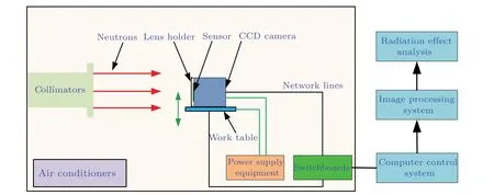
Fig.1.Schematic diagram of the irradiation experiment.
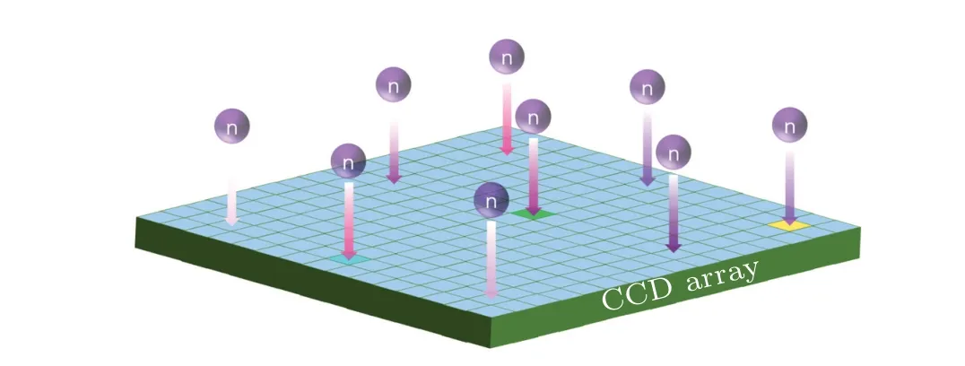
Fig.2.Schematic diagram of neutrons incident vertically upon the surface of the CCD array.Arrows with different color depths represent neutrons with different energies.Three pixels with different bright colors represent pixels that are damaged to different degrees after neutron irradiation.
3.Results and discussion
3.1.Hot pixels
The hot pixel represents the pixel of the image sensor,which has a larger leakage current.The position of the hot pixel is persistent and occurs at fixed positions on the output signal of the CCD.The proportion of hot pixels will have a great effect on the image quality of the imaging system, especially when used in a low-light environment with a long integration time.The leakage current will simply lighten up the pixel even with no light for a longer integration time.The large leakage current of the pixel is mainly induced by bulk defects in the sensitive volume of the CCD.Bulk defects can be induced in chip-making processes[14,15]or by particles in the radiation environment.[16,17]Only a few pixels are regarded as hot pixels before irradiation.After neutron irradiation, many bulk defects are produced in the sensitive volume of pixels,which will increase the leakage current and allow a normal pixel to become a hot pixel.Therefore, hot pixels are part of the CCD even if the device is not irradiated.
As stated in the EMVA 1288 standard,[13]it is not possible to find a common denominator to exactly define when a pixel is defective and when it is not.It is hard to find equally precise and quantitative definitions of hot pixels.Normally,a hot pixel is regarded as a pixel with a dark current two to four times greater than that of a normal pixel.In this paper,a pixel that has a dark current higher than twice the mean dark current of the normal pixel is considered to be a hot pixel.
Figure 3 shows normalized hot pixel counts of the CCD versus neutron irradiation fluence.From Fig.3, normalized hot pixel counts of the CCD increase with increasing neutron irradiation fluence.Figure 4 provides a three-dimensional surface plot of the experimental images (a) before radiation, (b)for a neutron radiation fluence of 1×10¹⁰neutron·cm−2, (c)for a neutron radiation fluence of 2×10¹⁰neutrons·cm−2and(d)for a neutron radiation fluence of 3×10¹⁰neutrons·cm−2.From Fig.4, we can see that many dark signal spikes appear in the images.Figure 5 shows the output signal of four pixels of the CCD versus irradiation time.The output signal is measured when the CCD is under neutron irradiation.From Fig.5, we can see that pixel3 [223,3] is damaged when the accumulated neutron fluence is about 5×10⁹neutrons·cm−2.However, when it is irradiated again at nearly 1700 s a little displacement damage appears.As for pixel2[27,4]and pixel4[131,3], a little displacement damage appears after an accumulated neutron fluence of about 5×10⁹neutrons·cm−2even though they are irradiated again at nearly 1700 s.As for pixel1[26,1], a little displacement damage appears after the accumulated neutron fluence reaches about 5×10⁹neutrons·cm−2.However,when it is irradiated again at nearly 1700 s the pixel is twice damaged by the neutrons and reaches the saturation state.We can also see that the output signal induced by the displacement damage displays the trend of a sudden, yet permanent,jump increase in the dark signal,mainly due to a single neutron collision event.The displacement damage effect on pixel1 [26,1] can also be called single-particle displacement damage.The RTS is observed in pixel1 [26,1].Transient response signals,which are not permanent displacement damage,induced by ionization can also be observed in Fig.5.
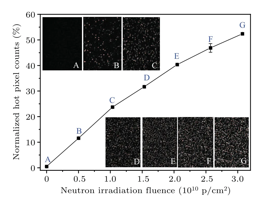
Fig.3.Normalized hot pixel counts versus neutron irradiation fluence.
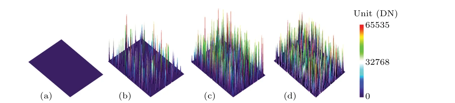
Fig.4.Three-dimensional surface plot of experimental images: (a) before irradiation, (b) neutron radiation fluence 1×10¹⁰ neutron·cm−2,(c)neutron radiation fluence 2×10¹⁰ neutrons·cm−2,(d)neutron radiation fluence 3×10¹⁰ neutrons·cm−2.

Fig.5.Output signal versus irradiation time.The red circles represent the transient signal, and the insert shows an enlarged image of the output signal of pixel 1.The numbers in [] represent the column and row number of the pixel.
When a neutron passes through the CCD two kinds of defects may be produced.One is a point defect, the other is a cluster defect.The defect type mainly depends on the energy of the second particle produced by neutrons interacting with the CCD.When the energy is high enough,cascade collisions will occur and clusters are produced.Otherwise, only point defects will be produced.Both point defects and clusters can become centers for the generation/recombination (G/R)of electron–hole pairs, carrier trapping and compensation of donors or acceptors,leading to an increase in the dark signal.
3.2.RTS
The RTS is a phenomenon whereby the dark signal switches randomly between two or more discrete states.The RTS in a sensor represents the fluctuation with time of the dark signal in the pixels.This phenomenon can be observed as pixel blinking in a series of dark images.The RTS will have a great effect on dark current calibration strategies and noise performance.[18]A typical RTS in a CCD induced by neutron irradiation is shown in Fig.6.The integration time is about 100 ms, and the irradiation fluence is about 3.07×10¹⁰neutrons·cm−2.From Fig.6 we can see that the RTS is very low when pixels are not irradiated by neutrons.However, after being irradiated by neutrons, a pixel that is hardly damaged by neutrons will produce the RTS phenomenon.The dark signal fluctuates dynamically with time.Some regularity can be found in Fig.6.For example, the dark signal of pixel9[25,189]appears at three dark signal levels, and is called a three-level RTS signal.The dark signal of pixel7 [62,7] appears at more than three dark signal levels, and is called multi-level RTS.The RTS is known to have two primary causes: the mobility of carriers is changed when charge carriers are trapped or emitted by traps in the gate oxide,and the number of carriers is changed when charge carriers are trapped or emitted by metastable Shockley–Read–Hall(SRH)G/R centers.After neutron irradiation,there are many bulk defects produced in the space charge region of the CCD which will become SRH G/R centers and produce the RTS phenomenon.Either two-level or multi-level RTS can be produced by a single event collision.Irradiation-induced clusters or complexes may be responsible for the two-level or multilevel RTS, and further work will be needed to confirm this hypothesis.[19]
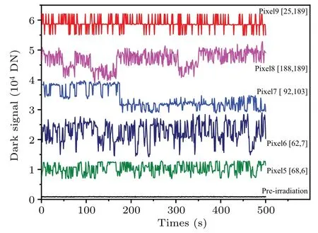
Fig.6.Typical RTS in the CCD pre-and post-neutron irradiation.
3.3.Mean dark signal
The mean dark signal is one of the most important radiation-sensitive parameters of the CCD.It can be used to evaluate the degree of degradation of the CCD after neutron irradiation.It represents the mean output signal of the pixel array in the dark environment without the injection of other signals.After neutron irradiation,many bulk defects are generated in the sensitive volume of the CCD,which will lead to an increase in dark signal or dark current.
According to the EMVA 1288 standard,the dark signal is given as follows:[13]
whereµdis the dark signal at a given integration time (texp),µd.0is the dark signal for zero integration time,µI.yis the dark current andtexpis the integration time.The mean dark signal over allM×Npixels is given as follows:
wheremandnare the row and column indices of the array.The mean dark signal versus integration time pre- and post-neutron irradiation is presented in Fig.8.From Fig.8,we can see that the mean dark signal increases with increasing integration time at the same irradiation fluence; the mean dark signal also increases with increasing irradiation fluence at the same integration time.From Fig.8, we can also see that the mean dark signal appears to be approximately proportional to irradiation fluence when the integration time is lower at the same irradiation fluence.However, when the integration time is higher,many damaged pixels reach saturation and the dark signal becomes constant with increasing integration time.Therefore,growth of the dark signal will decrease with increasing integration time.If the irradiation fluence and integration time are big enough,all the pixels will reach saturation and the mean dark signal will become constant with increasing integration time.

Fig.7.Mean dark signal versus integration time pre-and post-neutron irradiation.
The dark currentµI,darkcan be calculated according to the relationship between the mean dark signal and integration time in Fig.7.The dark current is equal to the slope of the straight line as shown in Fig.7.The unit of the dark current is given in DN·s−1or electrons·s−1(DN is the unit of the gray value of the out of image data).The dark current versus neutron irradiation fluence is shown in Fig.8.From Fig.8,we can see that the dark current appears to be approximately proportional to the irradiation fluence and the goodness-of-linear fit of experiments is aboutR2=0.988, which agrees with the universal damage factor(UDF)model introduced by Srour.[20]

Fig.8.Dark current versus neutron irradiation fluence.
3.4.DSNU
Neutron irradiation affects not only the mean dark signal but also the DSNU.The DSNU represents the non-uniformity of a dark image, which originates from the different output charge signals from one pixel to another in image sensors.The DSNU is given as follows:
The number of pixels that are damaged by incident neutrons exerts a great influence on the DSNU of image sensors.DSNU versus integration time pre- and post-neutron irradiation is shown in Fig.9.From Fig.9 we can see that the DSNU increases as the integration time increases at the same irradiation fluence.The DSNU also increases as the irradiation fluence increases at the same integration time.The hot pixels will have a great effect on the DSNU of the CCD.After neutron irradiation, many hot pixels are produced, making the DSNU increase dynamically.Moreover, DSNU2is linear with neutron irradiation fluence when the irradiation fluence ranges from 0 to 2.57×10¹⁰neutrons·cm−2at 100–460 ms, as shown in Fig.10.From Figs.4 and 9 we can see that the DSNU of the CCD is lower that that of the irradiated ones.Therefore, the ∆DSNU value is nearly the same as the DSNU.As has been described in our previous research work on the effects of neutron irradiation on the ∆DSNU of CMOS image sensors, ∆DSNU2is linear with neutron irradiation fluence.[10]The mechanism of the irradiation-induced increase in DSNU of the CCD is similar to that of a CMOS image sensor.Therefore, DSNU2is linear with neutron irradiation fluence,and the goodness-of-linear fitR2is better than 0.989.However,DSNU2will not be linear with neutron irradiation fluence when the irradiation fluence and integration time are sufficiently high,which will lead to many pixels reaching saturation.

Fig.9.DSNU versus integration time pre-and post-neutron irradiation.

Fig.10.DSNU2 versus integration time pre-and post-neutron irradiation.
4.TCAD simulation and discussion
In order to analyze the mechanisms of the effects of neutron displacement damage on the CCD, TCAD simulations were performed.Figure 11(a)shows the TCAD model of the CCD structure and the net doping.Figure 11(b) shows the potential distribution in the CCD under the normal base condition.The CCD device consists of a storage node,transfer node and drain node.There is an n-type active region at the surface above a p-type substrate.The drain node is used to deplete the electrons in the space charge region under the storage gate and transfer gate.In order to analyze the displacement damage induced by the neutrons,radiation damage effects are modelled by means of multi-level defect energy models and deep-level traps in n-type and p-type silicon are added to the structure of the CCD according to trap information in Ref.[21].The model is based on generalized SRH recombination statistics that are applied to the case of radiation-induced trap levels.The SRH recombination term is modified as follows:
whereRis the SRH recombination rate,RDandRAare the acceptor defect and donor defect recombination rates,lis the number of donor-like defects andmis the number of acceptorlike defects.
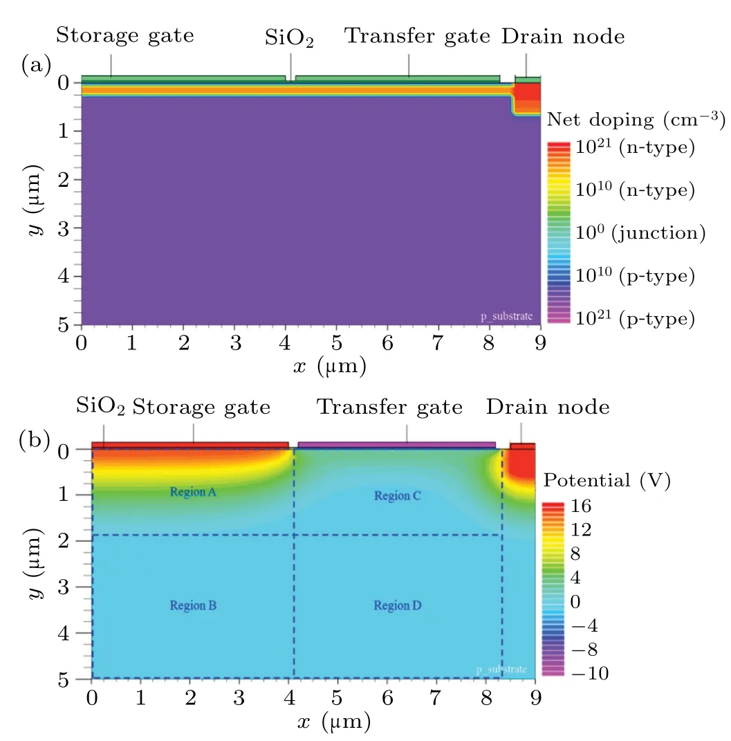
Fig.11.(a) TCAD models of the CCD structure and the net doping.(b)The potential distribution in the CCD(region A represents the space charge region under the storage gate, region B represents the substrate region under the storage gate,region C represents the region under the transfer gate and region D represents the substrate region under the transfer gate).
The output signal of the CCD is related to the concentration of electrons in the space charge region, and detailed information can be found in EMVA1288.[13]The relationship between the dark signal(µd)and the number of electrons(µd,e)can be written as
whereKis the overall system gain.To analyze the effect of irradiation on the typical parameters of a CCD,as we have described in Section 3,the average of the electron concentration in the space charge region is calculated under the different irradiation fluences.The average electron concentration in the space charge region of the CCD under the different irradiation fluences is shown in Fig.12 and the distribution of electron concentration under the different irradiation fluences is shown in Fig.13.From Fig.12 one can see that, according to the data fitting to the experimental findings, the linearity is up to 0.9995,which indicates a linear relationship between electron concentration in the space charge region and the irradiation fluence.These results also agree with our experimental results described in Section 3.

Fig.12.The average electron concentration in the space charge region of the CCD under different irradiation fluences.
To analyze the sensitive region of the displacement damage, traps are added in four regions in turn, as shown in Fig.11(b).Region A represents the space charge region under the storage gate.Region B represents the substrate region under the storage gate.Region C represents the region under the transfer gate(the region volume is the same as region B).Region D represents the substrate region under the transfer gate.The distribution of electron concentration in the space charge region of the CCD before irradiation,traps added in region A,traps added in region B,traps added in region C,traps added in region D and traps added in all four regions are plotted in Fig.14.The distribution of electron concentration is calculated when the integration time is about 10 ms.The trap density is calculated according to the data in Ref.[21]and the irradiation fluence is about 5×10¹⁴neutrons·cm−2.It can be seen that traps added in region A have more serious effects than those added in other regions.In order to quantify radiationinduced trap effects on the dark signal of the CCD,the proportional increase in electrons in the space charge region induced by traps in different regions is shown in Fig.15.It can be seen from the figure that nearly 80%of the increase in elections in space charge region is induced by the traps in region A when the irradiation fluence is no more than 5×10¹⁴neutrons·cm−2.Meanwhile,nearly 16%of the increase in elections is induced by the traps in region B and nearly 4%by the traps in region C.There is little effect of traps in region D.The traps induced by neutron irradiation can act as electron generation centers.The electrons generated in region A will be collected in the space charge region, which will lead to an increase in electron concentration.Besides, some of the electrons generated in regions B and C, which are near to region A, will also be collected through diffusion.

Fig.13.Device simulation of the distribution of electron concentration: (a) before irradiation; (b) fluence 1011 neutrons·cm−2; (c) fluence 1012 neutrons·cm−2,(d)fluence 1013 neutrons·cm−2,(e)fluence 1014 neutrons·cm−2 and(f)fluence 5×10¹⁴ neutrons·cm−2.
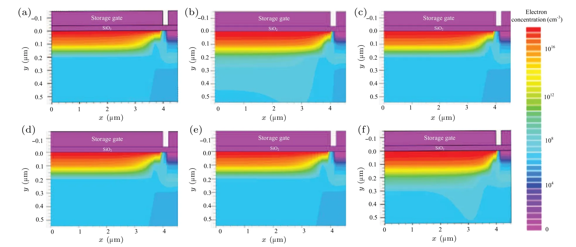
Fig.14.Device simulation of the distribution of electron concentration: (a)before irradiation;(b)traps added in region A;(c)traps added in region B;(d)traps added in region C;(e)traps added in region D;(f)traps added in all four regions.

Fig.15.The proportion of increased electrons in the space charge region induced by traps in different regions: (a) fluence 5×10¹⁰ neutrons·cm−2;(b)fluence 5×10¹² neutrons·cm−2;(c)fluence 5×10¹⁴ neutrons·cm−2.
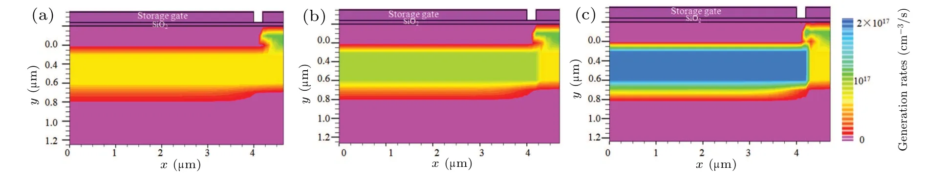
Fig.16.Device simulation of the generation rate distribution: (a) before irradiation; (b) fluence 1014 neutrons·cm−2; (c) fluence 5×10¹⁴ neutrons·cm−2.
Figure 16 shows the generation rate distribution under the different irradiation fluences when the traps are only added in region A.The generation rate is calculated according to the recombination rate.From Fig.16 one can see that the generation rate increases with increase in the irradiation fluence.The increase in the generation rate will increase the electron concentration in the space charge region of the CCD,leading to an increase in the dark signal of the CCD pixel.
5.Conclusion
This paper reports the effect of displacement damage on a CCD induced by neutrons at Back-n in the CSNS in an online irradiation experiment.The degradation mechanisms of the hot pixel, RTS, mean dark signal and DSNU induced by neutron irradiation are presented.
After neutron irradiation,many bulk defects are produced in the space charge region of CCD pixels,which will increase the leakage current and let normal pixels become hot pixels.Owing to point defects or clusters induced by neutron irradiation, two-level or multi-level RTS of hot pixels can be observed.The trends of hot pixels, mean dark signal, dark current and ∆DSNU2degradation are mainly linear with integration time and irradiation fluence.The mean dark signal, dark current and DSNU2will deviate from the linear relation obviously when many pixels reach saturation.According to our TCAD simulation there is a linear relationship between electron concentration in the space charge region and irradiation fluence when a pixel is far from saturation,which also agrees with our experimental results.Moreover, the dark signal induced by neutron irradiation is mainly caused by traps generated in the space charge region of the CCD, which will increase the generation rate of electrons.
More experiments and simulations need to be carried out to analyze the displacement damage effects on the CCD induced by neutrons at Back-n in the CSNS.The difference in the effects of radiation on CCD devices between single-energy neutrons and white neutron irradiation should also be investigated.
Acknowledgements
The authors are grateful to Jingyu Tang, HantaoJin,Zhixin Tan and Ruirui Fan of the Institute of High Energy Physics, Chinese Academy of Sciences for their useful support of this work.
Project supported by the Foundation of State Key Laboratory of China (Grant Nos.SKLIPR1903Z, 1803) and the National Natural Science Foundation of China (Grant Nos.U2167208 and 11875223).
猜你喜欢
杂志排行

Chinese Physics B的其它文章
- Interaction solutions and localized waves to the(2+1)-dimensional Hirota–Satsuma–Ito equation with variable coefficient
- Soliton propagation for a coupled Schr¨odinger equation describing Rossby waves
- Angle robust transmitted plasmonic colors with different surroundings utilizing localized surface plasmon resonance
- Rapid stabilization of stochastic quantum systems in a unified framework
- An improved ISR-WV rumor propagation model based on multichannels with time delay and pulse vaccination
- Quantum homomorphic broadcast multi-signature based on homomorphic aggregation