Controlled vapor growth of 2D magnetic Cr2Se3 and its magnetic proximity effect in heterostructures∗
2021-09-28DanliangZhang张丹亮ChenYi易琛CuihuanGe葛翠环WeiningShu舒维宁BoLi黎博XidongDuan段曦东AnlianPan潘安练andXiaoWang王笑
Danliang Zhang(张丹亮),Chen Yi(易琛),Cuihuan Ge(葛翠环),Weining Shu(舒维宁),Bo Li(黎博),Xidong Duan(段曦东),Anlian Pan(潘安练),and Xiao Wang(王笑),§
1School of Physics and Electronics,Hunan University,Changsha 410082,China
2Key Laboratory for Micro-Nano Physics and Technology of Hunan Province,College of Materials Science and Engineering,Hunan University,Changsha 410082,China
3Hunan Key Laboratory of Two-Dimensional Materials and State Key Laboratory for Chemo/Biosensing and Chemometrics,College of Chemistry and Chemical Engineering,Hunan University,Changsha 410082,China
Keywords:Cr2Se3,magnetic proximity effect,heterostructures
1.Introduction
The emerging two-dimensional(2D)magnetic materials provide an ideal system for both basic physics and spintronic applications due to their unique 2D-limited magnetism and spin states on the nanomater scale.[1–3]Combining 2D magnetic and non-magnetic(semiconductor)materials can form a new type of Van der Waals(vdW)heterostructures,in which the so called magnetic proximity effect could play an import role.The effect is highly sensitive to the interfacial electronic properties and has opened up new opportunities to manipulate spintronics,superconductivity,excitonic and topological phenomena.[4]The manipulation of spintronics and valleytronics in 2D vdW heterostructures using the magnetic proximity effect has been demonstrated,manifesting an enhanced valley Zeeman splitting and/or modifications of the valley polarization.[4–10]
The controllable realization of high-quality 2D magnetic materials is crucial for the investigation of the magnetic proximity effect and also potential device applications.2D magnetic materials,such as Fe3GeTe2,Cr2Ge2Te6,CrI3atomic layers,are mainly obtained via the mechanical exfoliation from their bulk counterparts,[11–14]which has difficulties in controlling the thickness,domain size and the obtained layers are relatively unstable in air.Recently,the wafer-scale thin films of Fe3GeTe2were obtained via a molecular beam epitaxy(MBE)method,which could promote the realization of practical devices.[15]In contrast,2D non-layered materials have strong chemical bonds instead of Van der Waals interaction among the layers,therefore,they are hard to obtain via the mechanical exfoliation method.Chemical vapor deposition(CVD)route has been utilized to prepare air-stable and large size nonlayered magnetic materials such as Cr2S3,CrSe,and Cr2Te3,which exhibit excellent optical,electrical,and magnetic properties.[16–20]Such materials with different stoichiometry can be obtained by controlling the growth conditions,such as deposition temperature,carrier gas,and source ratio.[21–23]Very recently,bulk chromium selenium(Cr2Se3)was obtained experimentally and the crystal structure and magnetic properties were investigated as well.[24]However,ultrathin 2D Cr2Se3nonlayered magnetic materials and the related photophysics have not yet been explored.Moreover,Cr2Se3-based vdW heterostructures of related magnetic applications in spintronics and valleytronics are desirable to be explored.
In this work,we realize the synthesis of thicknesstunable and air-stable rhombohedral single-crystal Cr2Se3via the CVD method.Single-unit-cell thick(≈1.8 nm)Cr2Se3nanosheets and thicker nanosheets with a lateral length of 120µm are successfully obtained.By constructing vdW magnetic heterostructures with ultrathin 2D Cr2Se3nanosheets and monolayer WS2,we investigate the magnetic proximity effect in the heterostructures and the related manipulation of spin and valley pseudospin in monolayer WS2.Our findings contribute to the controlled growth of new 2D magnetic materials and the understanding and utilization of magnetic proximity effect.
2.Experimental details
The growth of Cr2Se3nanosheets was carried out in a single-temperature-zone tube furnace by a CVD route(Fig.1(a)).A ceramic boat with selenium(Se)powder(99.9%,Alfa)was placed in the upstream area of the tube furnace.The mixed powders of chromium(Cr;99%,Alfa)and sodium chloride(NaCl;99.99%,Alfa)with a weight ratio of 10:1 were loaded in the other ceramic boat,and a fresh and clean growth substrate(fluorophlogopite([KMg3(AlSi3O10)F2])mica,300 nm-SiO2/Si or glassy silica substrate)was placed directly above it.The ceramic boat was placed in the central heating zone of the tube furnace.Notably,the NaCl powder was used to lower the melting point of the Cr powder(melting point is 1857°C)and the energy barrier as well as to increase the reaction rate.[25,26]The temperature of the tube furnace was increased from room temperature to 820–900°C within 25–30 min with the Ar flow rate of 60 sccm,and the furnace temperature was maintained for 3–5 min for sample growth.Finally,the Cr2Se3nanosheets with different thicknesses were obtained.The results suggest that the fluorophlogopite mica substrate with chemically inert surface and atomic flat is conducive to the epitaxial growth of thinner Cr2Se3samples.[27]
For constructing the heterostructure,the monolayer WS2exfoliated from their bulks was transferred to the thin Cr2Se3nanosheet surface by the PDMS-assisted dry transfer method.To enhance the coupling of the heterostructures interface,the WS2/Cr2Se3heterostructure sample was placed in a vacuum annealing furnace set at 180°C for 8 hours.
To further understand the morphology and atomic structure,the CVD-synthesized Cr2Se3nanosheets were characterized via optical microscope(Axio Scope A1,Zeiss),atomic force microscope(AFM,Multimode 8,Bruker),x-ray diffraction(XRD,MiniFlex 600,Rikaga),x-ray photoemission spectroscopy(XPS,250Xi,ESCALAB),scanning electron microscope(SEM,SIGMA HD,Zeiss),and transmission electron microscopy(TEM,Tecnai G2-20,FEI).High-resolution TEM(HRTEM)and selected area electron diffraction(SAED)measurements were also performed to identify the atomic structure and crystallinity of the triangle-shaped Cr2Se3nanosheets.The physical property measurement system(PPMS,Dyna-Cool 9,Quantum Design)was used to measure the magnetic properties of the CVD grown samples.
Raman spectroscopy of the Cr2Se3nanosheets was performed by a confocal optical microscope(WITec,alpha-300)under the excitation of a continuous wave laser at 532 nm.Circular polarization-resolved photoluminescence(PL)spectroscopy was recorded with a 488 nm laser,and the optical path and experimental details are the same as reported in our previous studies.[28,29]It is worth noting that in this study we always collected the PL emission with the same circular polarization as that of the excitation.We define the PL degree of circular polarization(ρ)asρPL=(Iσ+/σ+−Iσ−/σ−)/(Iσ+/σ++Iσ−/σ−),where Iσ+/σ+(Iσ−/σ−)represents the PL intensity under bothσ+(σ−)excitation andσ+(σ−)detection.
3.Results and discussion
Based on the described growth method,we successfully prepared thickness controllable 2D Cr2Se3nanosheets.The non-layered Cr2Se3single crystal displays the single-unit-cell with abc stacking sequence and the thickness of about 1.8 nm(Fig.1(b)).The top and side views of the Cr2Se3crystal structure are shown in supporting information Fig.S1.Figure 1(c)displays the AFM image of the CVD-synthesized Cr2Se3nanosheet obtained from a mica substrate showing a smooth surface with a thickness of about 1.8 nm,which corresponds to the one-unit-cell thickness of Cr2Se3.To control the thickness of grown Cr2Se3,we precisely controlled the heating temperature while keeping other growth parameters(such as growth time,gas flow)constant during the CVD growth process.Figure 1(d)shows typical optical images of Cr2Se3grown on mica substrate at different growth temperatures.It is clear that the Cr2Se3nanosheets evidently grow thicker and larger with increasing the temperature.The corresponding thickness varied from~1.8 nm to tens of nanometers confirmed by the AFM measurement,when the temperature was increases from 820°C to 900°C.We also tested the stability of the CVD-synthesized Cr2Se3.According to the AFM image,we observed no obvious changes from the nanosheet after 283 days(supporting information Fig.S2).Figure 1(e)shows the optical image of a large area thicker non-layered Cr2Se3(approximately 10 nm)grown on mica.Hexagon and triangle-shaped Cr2Se3nanosheets distribute throughout the substrate.The inset of Fig.1(e)shows the Cr2Se3nanosheet with a lateral length of 120µm.In order to explore the influence of the substrate on growth,the 300 nm-SiO2/Si and glassy silica substrates were used as well.The Cr2Se3tends to grow triangle-shaped samples on the 300 nm-SiO2/Si and glassy silica substrates(Figs.1(f)and 1(g)).To explore the crystal vibrational properties,Raman spectroscopy was used to measure the Cr2Se3nanosheets.The Raman spectra of the as-grown Cr2Se3nanosheets on the mica substrate with different thicknesses varying from 6 nm to 26 nm were collected(Fig.1(h)).The Raman mode at 253 cm−1redshifts as the thickness increases,showing a clear thickness dependence.The two characteristic Raman peak mappings extracted from the integrated intensities of 145 cm−1and 253 cm−1indicate uniform crystallinity under 532 nm laser excitation(supporting information Figs.S3a and S3b).
The XRD was used to investigate the crystal structure of the CVD-synthesized Cr2Se3nanosheets on SiO2/Si substrate(Fig.2(a)).The observed four prominent diffraction peaks well match the standard PDF card(PDF#89-2068)from the rhombohedral Cr2Se3of[001]crystal plane.Based on the XRD data,the crystal structure geometry of Cr2Se3belongs to the space group R¯3 with the lattice constants of a=b=6.254˚A and c=17.382˚A,which is consistent with the previous studies.[24,30]To determine the chemical states and elemental composition,the CVD-grown sample was measured by XPS(Figs.2(b)and 2(c)).The two doublet peaks in the Cr 2p spectra correspond to the chemical states of Cr 2p1/2and 2p3/2,with the first pair locating at 584.0 eV and 574.5 eV,while the second pair appearing at 586.2 eV and 576.8 eV attributed to the satellite peaks.In the Se 3d spectra(Fig.2(c)),the peaks at around 55.3 eV and 54.2 eV represent the Se 3d3/2and 3d5/2,respectively.For the transmission electron microscopy characterization,the asgrown samples on the SiO2/Si substrate were transferred to the carbon-supported copper grid via the PMMA-assisted transfer route.[31]Figure 2(d)shows the HRTEM image of Cr2Se3with a clear hexagonal atomic arrangement,extracted from which the(110)crystal plane spacing is about 0.31 nm.Figure 2(e)shows the corresponding SAED pattern with the six equivalent diffraction spots from the(110)lattice planes.The existence of one set of spots in the SAED pattern demonstrates the single crystal nature of the Cr2Se3.The inset of Fig.2(e)shows the low-magnification TEM image of the Cr2Se3nanosheet.The elemental composition of the synthesized Cr2Se3crystals can be further analyzed by energy-dispersive spectroscopy(EDS)spectroscopy.The Cr:Se atomic ratio is calculated to be 38.6:61.4,close to 2:3 through the computation of peak areas,confirming the formation of stoichiometric hexagonal phase Cr2Se3(Fig.2(f)).[30,32]Figure 2(g)shows the representative SEM image of the Cr2Se3nanosheet on mica substrate.The Cr2Se3nanosheet is smooth and clean across the whole sample region.The corresponding SEM elemental mappings are shown in Figs.2(h)and 2(i).Based on the SEM results,we can confirm that the synthesized Cr2Se3nanosheets consist of uniform distributed Cr and Se elements.The atomic ratio of Cr and Se elements is 38.76:61.24,similar as the data from EDS,which further confirms the composition information of the sample.Similar SEM results were obtained from the samples grown on glassy silica and SiO2/Si substrates(supporting information Fig.S4).There is no obvious difference in the structure and properties of the samples grown on these three substrates.The high-quality Cr2Se3sample enables it as an ideal candidate for further research and applications,especially for designing novel spintronics and valleytronics with simpler structures.
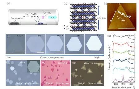
Fig.1.(a)Schematic illustration of the CVD growth process of Cr2Se3 nanosheets,gray:Se powder,blue:Cr,yellow:NaCl powder.(b)Structural model of the Cr2Se3 crystal.(c)AFM image of the triangle-shaped Cr2Se3 with the thickness of 1.8 nm(one-unit-cell).(d)Growth-temperature dependent bright-field optical images of as-grown Cr2Se3 nanosheets under growth conditions of 820–900 °C over 25 min.(e)–(g)Typical brightfield optical images of Cr2Se3 nanosheets on(e)mica,(f)SiO2/Si,and(g)glassy silica substrates.The inset of(e)shows a Cr2Se3 nanosheet with a lateral length of 120µm.(h)Raman spectra of the Cr2Se3 nanosheets with different thicknesses.All scale bar:20µm..
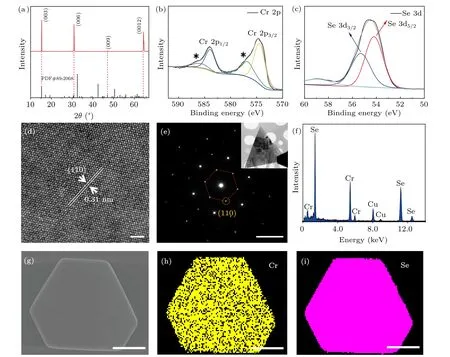
Fig.2.(a)XRD spectra of thicker Cr2Se3 nanosheets.(b),(c)XPS spectra from Cr 2p peaks and Se 3d peaks of the Cr2Se3 nanosheets.(d)HRTEM image of the Cr2Se3 nanosheet;scale bar:2µm.(e)The corresponding SAED patterns of the Cr2Se3 nanosheet;scale bar:5 nm−1.The lowmagnification TEM image of the Cr2Se3 nanosheet is shown in the inset.(f)EDX spectrum of the Cr2Se3 nanosheet.(g)SEM image of a Cr2Se3 nanosheet and its corresponding SEM elemental mappings of Cr(h)and Se atoms(i).Scale bar:3.5µm.
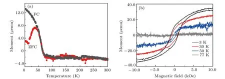
Fig.3.(a)The temperature dependent magnetization of Cr2Se3 nanosheets on SiO2/Si substrate under a parallel magnetic field of 1000 Oe.The ZFC process is represented by the red curve;the FC process is represented by the gray curve.(b)Magnetic hysteresis loop from the Cr2Se3 nanosheets at different temperatures with a parallel magnetic field.
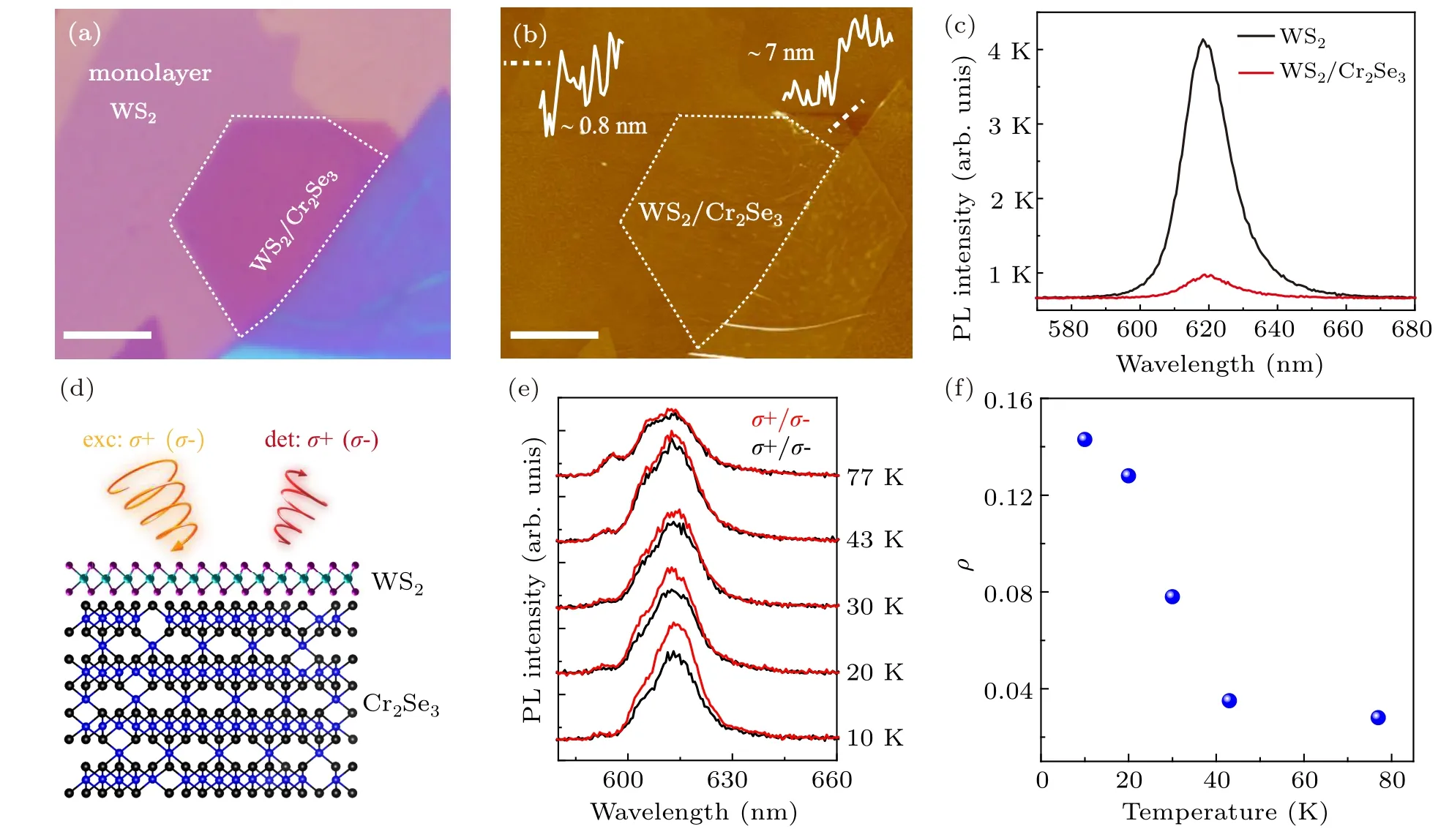
Fig.4.(a)Bright-field optical image of the WS2/Cr2Se3 heterostructure on SiO2/Si substrate.(b)The corresponding AFM image with height profile of the sample in(a).(c)Typical PL spectra from the WS2/Cr2Se3 heterostructure region and bare monolayer WS2,respectively.(d)Schematic illustration of the polarization experiments for the WS2/Cr2Se3 heterostructure.Only the PL emission with the same circular polarization as the excitation was collected.(e)Circularly polarized PL spectra of the WS2/Cr2Se3 heterostructure at different temperatures.(f)The temperaturedependentρof the monolayer WS2 PL from the heterostructure.
To identify the magnetic properties of the CVDsynthesized Cr2Se3samples,almost film-forming Cr2Se3samples with a thickness up to micron on the SiO2/Si substrate were investigated by a physical property measurement system.Figure 3(a)shows the temperature-dependent magnetic moments under the parallel magnetic field of 1000 Oe,which shows the obvious magnetic properties of the CVDsynthesized Cr2Se3.The zero-field-cooled(ZFC)and fieldcooled(FC)curves show the magnetic transition temperature at about 75 K and indicate a net magnetic moment below the magnetic transition temperature,which is consistent with the previous reports.[24,33]Furthermore,the temperature dependent magnetic hysteresis loops under the parallel magnetic field scanning within±1 T are shown in Fig.3(b).The results show that there is obvious magnetic hysteresis at the temperature range from 3 K to 77 K.According to the previous studies,the out-of-plane hysteresis of Cr2Se3crystals is much stronger than that of in-plane.[24]The obvious magnetic properties of the CVD-grown Cr2Se3nanosheets provide a good opportunity for the manipulation of spin/valley physics.
To further investigate the magnetic proximity effect of the CVD-grown Cr2Se3nanosheets,the van der Waals heterostructures consisting of a bottom ultrathin CVD-grown Cr2Se3nanosheet and a top mechanically exfoliated monolayer WS2were fabricated with the dry transfer method,which was operated under ambient condition.There is no further encapsulation for the heterostructures.Monolayer WS2with rich pseudospin and valley degrees of freedom is a typical nonmagnetic semiconductor,which can be manipulated using circularly polarized light.[28,29,34]The optical microscope image of the WS2/Cr2Se3heterostructure is shown in Fig.4(a),of which the heterostructure region is framed by white dashed lines.The corresponding AFM image(Fig.4(b))shows the top WS2and the bottom Cr2Se3with the thicknesses of about 0.8 nm and 7 nm,respectively.The relative thin layers could enable the magnetic proximity effect in the WS2/Cr2Se3heterostructures.Under linearly polarized laser excitation,typical PL spectra collected from the heterostructure region and that from the bare monolayer WS2are compared in Fig.4(c).The PL intensity of WS2from the WS2/Cr2Se3heterostructure region is significantly quenched compared to that of pure monolayer WS2,which is attributed to the transfer of carriers from the top monolayer WS2to the bottom Cr2Se3.The circular polarization-resolved PL measurements from the WS2/Cr2Se3heterostructure were further investigated,without introducing any additional magnetic dopants or field.Figure 4(d)schematically illustrates the circularly polarized light excitation and PL emission of the WS2in a WS2/Cr2Se3heterostructure.Theoretically,the±K valley is degenerate and the PL degree of circular polarizationρ=(Iσ+/σ+−Iσ−/σ−)/(Iσ+/σ++Iσ−/σ−)is zero without external magnetic field due to the time reversal symmetry.[35]However,since the monolayer WS2is adjacent to the magnetic Cr2Se3,ρis expected to have a larger value,and its sign should be directly related to the bottom Cr2Se3magnetization direction.[8]Figure 4(e)displays the temperature-dependent circularly polarized PL spectra of the WS2/Cr2Se3heterostructures.The valley degeneracy and time reversal symmetry of monolayer WS2are broken due to the adjacent 2D magnetic Cr2Se3.[4]The PL intensity under theσ+excitation andσ+detection(σ+/σ+,red curve)is always stronger than that of theσ−/σ−configuration(black curve),indicating the non-zero value ofρ.From the spectra shown in Fig.4(e),we calculatedρof the WS2PL in the WS2/Cr2Se3heterostructure at different temperatures and showed thatρdecreases from 14.3%to 2.8%as the temperature increases from 10 K to 77 K(Fig.4(f)).The circularly polarized PL spectra of the WS2/Cr2Se3heterostructures on glassy silica and mica substrates at 10 K show similar magnetic proximity effect induced valley polarization as the heterostructures grown on SiO2/Si(supporting information Fig.S5).This suggests that the observed temperaturedependent polarization may originate from the magnetic proximity effect by the optical control.[4,8,9]Our results demonstrated that the CVD-grown 2D Cr2Se3can efficiently manipulate the spin/valley physics in ambient atmosphere,which makes them promising for practical device applications.
4.Conclusion
In summary,we have successfully synthesized thicknesstunable Cr2Se3single crystal using a CVD method.We realized high-quality nonlayered Cr2Se3nanosheets with thickness down to one-unit-cell(≈1.8 nm)and also a larger lateral length size of about 120µm at a thicker thickness.According to crystal structure characteristics and related magnetic properties,we showed that the lattices structure of hexagonal phase Cr2Se3has a–b–c sequence in space group R¯3,with a magnetic transition temperature of approximate 75 K.Moreover,we have demonstrated the magnetic proximity effects in the WS2/Cr2Se3vdW heterostructure to manipulate the valley polarization of the adjacent WS2.Our work paves the way for potential applications in spintronic and valleytronic devices with novel 2D magnetic materials via the magnetic proximity effect.
杂志排行

Chinese Physics B的其它文章
- Multiple solutions and hysteresis in the flows driven by surface with antisymmetric velocity profile∗
- Magnetization relaxation of uniaxial anisotropic ferromagnetic particles with linear reaction dynamics driven by DC/AC magnetic field∗
- Influences of spin–orbit interaction on quantum speed limit and entanglement of spin qubits in coupled quantum dots
- Quantum multicast schemes of different quantum states via non-maximally entangled channels with multiparty involvement∗
- Magnetic and electronic properties of two-dimensional metal-organic frameworks TM3(C2NH)12*
- Preparation of a two-state mixture of ultracold fermionic atoms with balanced population subject to the unstable magnetic field∗