Trigger mechanism of PDSOI NMOS devices for ESD protection operating under elevated temperatures*
2021-07-30JiaXinWang王加鑫XiaoJingLi李晓静FaZhanZhao赵发展ChuanBinZeng曾传滨DuoLiLi李多力LinChunGao高林春JiangJiangLi李江江BoLi李博ZhengShengHan韩郑生andJiaJunLuo罗家俊
Jia-Xin Wang(王加鑫) Xiao-Jing Li(李晓静) Fa-Zhan Zhao(赵发展)Chuan-Bin Zeng(曾传滨) Duo-Li Li(李多力) Lin-Chun Gao(高林春) Jiang-Jiang Li(李江江)Bo Li(李博) Zheng-Sheng Han(韩郑生) and Jia-Jun Luo(罗家俊)
1Institute of Microelectronics,Chinese Academy of Sciences,Beijing 100029,China
2Key Laboratory of Science and Technology on Silicon Devices,Chinese Academy of Sciences,Beijing 100029,China
3University of Chinese Academy of Sciences,Beijing 100029,China
Keywords: ESD,trigger voltage,temperature,GGNMOS,GTNMOS,TCAD
1. Introduction
Electrostatic discharge (ESD) has been a threat to reliability in the semiconductor industry for decades. Novel ESD protecting devices are frequently designed to mitigate such concerns.[1-4]Meanwhile, high temperature is a typical environment for integrated circuits.[5,6]The assembly and operation of integrated circuits in some cases take place at elevated temperatures. Hence, The ESD protecting designs become more complicated due to the thermally-induced variations of ESD parameters,and it is necessary to systematically and comprehensively analyze the characteristics of ESD protecting devices to ensure that they are suitable for operating under elevated temperatures.Kooet al.[7]reported the features of the high holding voltage of the new silicon controlled rectifier (SCR) ESD protecting device at different temperatures and improved the stability in a temperature range of 25°C-225°C and made a detailed analysis. Meneghessoet al.[8]introduced a new type of SCR, the low-voltage-trigger SCR ESD protecting structure, and obtained a high holding voltage, and performed two-dimensional (2D) device simulation(DESSIS Synopsys)to obtain the temperature dependence of the holding voltage at 25°C-125°C.Lianget al.[9]introduced the temperature dependence of the critical parameters of a variety of typical SCR and diode structures at a temperature of 225°C. Liet al.[10]introduced the temperature dependence of diode and GGNMOS(grounded-gate NMOS)in a temperature range from-40°C to 110°C.Jang and Lin[11]and Janget al.[12]analyzed the temperature-dependent steady and dynamic state characteristics of SCR-based ESD protecting circuits,focusing on the triggering and holding behavior of ESD protecting devices. Houet al.[13]improved a thermal-stable diode-triggered silicon-controlled rectifier(TSDTSCR)device to obtain almost constant high-temperature ESD protecting capabilities. Doet al.[14]developed the floating technology to reduce the trigger voltage of 4H-SiC GGNMOS to cater to the design window and carried out high-temperature evaluation. Arbess and Bafleur[15]looked into a new type of MOS insulated gate bipolar transistor(MOS-IGBT)power clamping device for high-temperature operation. It had a lower temperature sensitivity at 200°C. However, in most of those studies considered are only the changes in the characteristics of the traditional or novel ESD protecting devices with temperature to verify their reliability within their operating temperature range, but the relation of temperature to triggering, or holding, or failure characteristics are not analyzed by the underlying physical mechanism and simulation.
In this paper,the temperature-dependent triggering characteristics of partially depleted silicon-on-insulator (PDSOI)NMOS devices for ESD protection are analyzed. The transmission line pulsing(TLP)I-Vcurves are measured, and the first breakdown voltage (VT1) is studied and discussed. The technology computer aided design(TCAD)simulation is carried out to obtain a physical insight into the mechanism of the temperature dependence of the triggering behavior.
2. Experiment
The device under test (DUT) was an H-gate NMOS device and fabricated with a 0.18-μm PDSOI technology. More parameters are summarized in Table 1. The measurements were targeted to the human body model(HBM)and conducted using the TLP/VFTLP(transmission line pulse/very fast transmission line pulse)test system HOXI-I with a pulse width of 100 ns and a rise time of 5 ns, which is made in the Institute of Microelectronics of the Chinese Academy of Sciences.The heating module provided a testing temperature range from 30°C to 200°C. We characterized the TLPI-Vcurves of the two operating modes, the grounded-gate NMOS (GGNMOS)mode and the gate-triggered NMOS(GTNMOS)mode,under varying temperatures. The GGNMOS mode describes an NMOS-based ESD protecting device whose gate, source,body, and substrate electrode were connected to the ground(0 V),and the drain electrode was subjected to the ESD stress.The GTNMOS differs from GGNMOS in an extra DC gate voltage supply. In our experiment, a 1.5-V DC voltage was applied to the gate electrode during the TLP testing in GTNMOS mode.
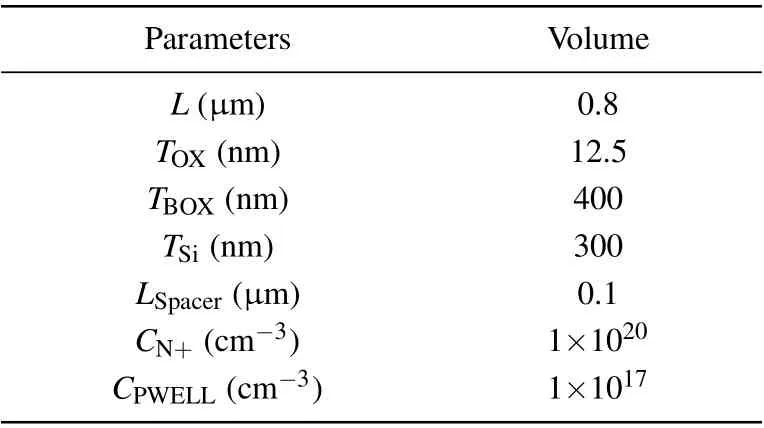
Table 1. Some parameters of the device under test.
Figure 1(a)shows the measured TLPI-Vcurves near the first breakdown point of the GGNMOS.The measured TLPIVcurves near the first breakdown point of the GTNMOS are presented in Fig. 1(b) as discussed in our previous work.[16]Each figure includes five curves related to the five different temperatures. The measured TLPI-Vcurves are normalized to the current per unit gate width,i.e.,each ESD current value is divided by the total width of the PDSOI NMOS device. The measurement results suggest that the values ofVT1of GTNMOS are all lower than those of GGNMOS.The value ofVT1in GGNMOS mode increases from 8.8 V to 9.7 V with temperature increasing from 30°C to 195°C.The total rise is about 0.9 V, accounting for 10.2 percent of room-temperatureVT1.In the GTNMOS mode,a 1.5-V voltage is applied to the gate electrode.The value ofVT1in GTNMOS mode decreases from 6.84 V to 6.11 V in a temperature range from 30°C to 195°C.The total decline is nearly 0.73 V,which is about 10.7 percent ofVT1at room temperature,The above results indicate that theVT1varies in an opposite trend with the increasing of temperature in the two modes. The mechanisms will be analyzed by TCAD simulation below.
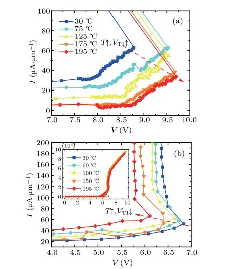
Fig. 1. TLP I-V curves of DUT in temperature range of 30 °C to 195 °C(near the first breakdown point)for(a)GGNMOS and(b)GTNMOS.
3. Simulation results
To support and analyze the experimental conclusion,TCAD simulation is carried out. The two-dimensional (2D)model for simulation is shown in Fig. 2, in which the body contact is set to be on the right of the source contact. Just because the body contact configuration of the 2D model is different from that in the real H-gate PDSOI NMOS device, the absolute value ofVT1in the simulation curve differs from that of the measured TLPI-Vcurve. Nevertheless,the same trend ofVT1versus temperature is obtained in the TCAD simulation, which is essential to analyze the trigger mechanism at high temperatures.
The simulation method is named the multi-current pulse simulation method.In the method,a customized piecewise linear function(PWL)is used to generate the TLP current pulse which is applied to the drain electrode.As shown in Fig.2,the DC voltages of 0 V and 1.2 V are applied to the gate electrode in GGNMOS and GTNMOS modes,respectively. Other electrodes including the source, body, and substrate electrode are connected to the ground(0 V).
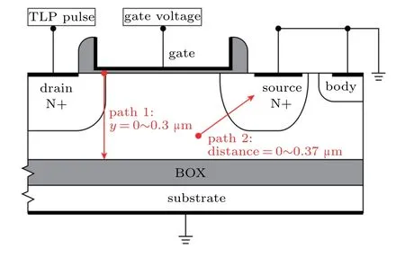
Fig.2. Schematic diagram of the 2D model.
Figures 3 and 4 show the simulated transientI-Vcurves of DUT operating in GGNMOS mode and GTNMOS mode,respectively. The variation ofVT1versustemperature of TLP testing and TCAD simulation are shown in Fig. 5. The simulation results suggest thatVT1increases with temperature increasing in GGNMOS mode and decreases in GTNMOS mode, which is consistent well with the measured TLPI-Vcharacteristics given in Figs.1(a)and 1(b).
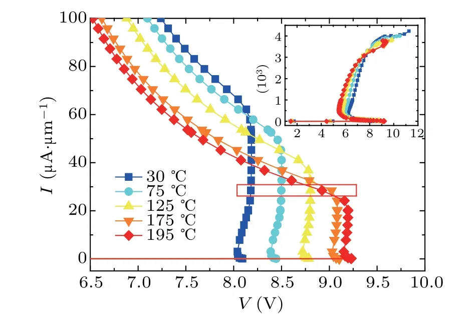
Fig.3. TCAD simulation I-V curves of GGNMOS at temperatures ranging from 30°C to 195°C near the first breakdown point,with inset showing overall simulation I-V curves of GGNMOS under five different temperatures.
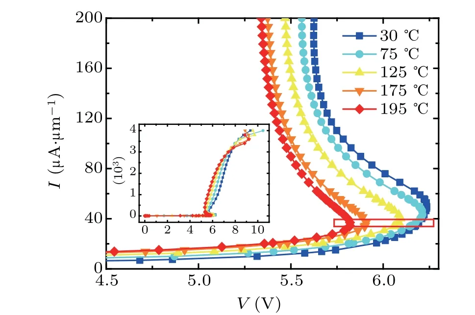
Fig.4. TCAD simulation I-V curves of GTNMOS at temperatures ranging from 30 °C to 195 °C near the first breakdown point, with inset exhibiting overall simulation I-V curves of GTNMOS under five different temperatures.
To analyze the underlying physical mechanism of the temperature dependence ofVT1in GGNMOS mode and in GTNMOS mode comparatively,we choose 5 points in each mode to analyze the response process under five operating temperatures as marked in Figs. 3 and 4. At each point, a certain moment in a range of 70%-90%of the TLP pulse period is selected to analyze the distribution of some essential parameters in the following.
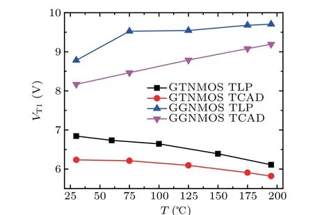
Fig.5. Variations of VT1 with temperature of TLP testing and TCAD simulation.
3.1. Discussion of GGNMOS
3.1.1. Electric field
Before the first breakdown point, the ESD current maintains a very low level and flows through the drain contact,reversed drain-body junction, body region, and the body contact.Because of the high resistance of the reversed drain-body junction, a relatively high ESD voltage is mostly clamped at the junction, thus forming an extremely high electric field.Therefore,the electric field distribution at the first breakdown point is an indication ofVT1. The electric field distribution along path 1 (marked in Fig. 2) is shown in Fig. 6. It can be seen that the electric field increases with temperature in GGNMOS mode and decreases in GTNMOS mode. The peak electric field of GGNMOS is about 1.5 times higher than that of GTNMOS.The relationship between the critical electric field,Ec,and the avalanche threshold voltage,Vava,is given by[17]
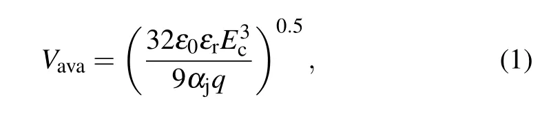
whereε0andεrare the permittivity of vacuum and the relative dielectric constant, respectively,αjrepresents the ionization rate of collision,andqdenotes the elementary charge.Equation (1) describes the avalanche mechanism in the linear graded PN junction. As temperature increases, the mean free path of the carriers in the space charge region decreases,a higherEcis needed for the carriers to obtain enough kinetic energy to trigger the avalanche breakdown. Thus, the thermal coefficient of the avalanche mechanism is proportional to temperature.[9,10]
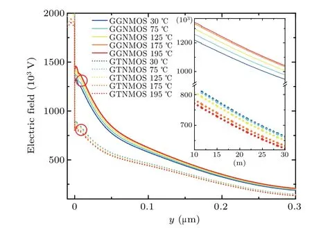
Fig.6. Electric field distributions in GGNMOS mode and GTNMOS mode along path 1 under various ambient temperatures.
In the GGNMOS mode,the triggering of the DUT relies on the avalanche breakdown of the drain-body junction. The avalanche multiplication generates a large number of electronhole pairs and the holes drift towards the body contact,which generates a voltage drop across the body resistanceRBodyand raises the local body potentialVBody. The source-body junction is turned on by enoughVBody, leading the parasitic BJT to trigger on. Thus, theVT1of GGNMOS is governed by the avalanche critical electric field and the avalanche threshold voltage in the drain-body junction,resulting in theVT1of GGNMOS increasing with temperature rising.
Oppositely, the decreasing ofVT1of GTNMOS suggests that there exist other prior triggering mechanisms besides the avalanche in GTNMOS mode.
3.1.2. Impact ionization
Impact ionization occurs when the high reverse bias voltage of the drain-body junction creates a strong internal electric field,which accelerates the carriers through the silicon crystal lattice and produces secondary electron-hole pairs. The impact ionization can be used to characterize the efficiency of avalanche multiplication for GGNMOS.
Figure 7 shows the impact ionization distributions at the drain-body junction under various ambient temperatures in GGNMOS mode and the GTNMOS mode, respectively. It can be seen in Fig.7 that the total impact ionization decreases with temperature increasing in both GGNMOS mode and GTNMOS mode.
The impact ionization is mainly governed by the electric field and the mean-free path of the carriers. As mentioned before,the critical triggering electric field increases with temperature increasing. Hence, the electric field with a positive temperature coefficient proves to influence the impact ionization little in the GGNMOS mode. The mean free path of the carriers is dominated by the scattering of phonons, generated by the vibration of the atomic lattice,which is positively correlated with temperature. The mean-free path is visualized by the mobility distribution,which decreases with temperature increasing as shown in Fig.8.
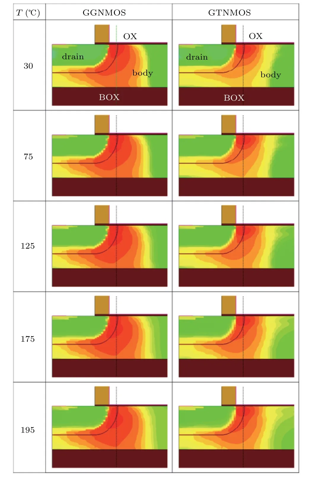
Fig. 7. Impact ionization distributions in GGNMOS mode and GTNMOS mode at drain-body junction under various ambient temperatures.
To sum up,the avalanche threshold voltage of the drainbody junction in DUT increases with temperature increasing because the impact ionization is inversely proportional to temperature. And it is the reason why theVT1in GGNMOS mode rises when the temperature goes up.
From Figs. 3 and 4 it follows that comparing with the GGNMOS mode,VT1of GTNMOS decreases with temperature increasing, which means that the first breakdown in the GTNMOS mode occurs at a lower electric field and lower impact ionization than in GGNMOS. Thus, the temperature dependence of triggering in GTNMOS mode is not governed by avalanche breakdown but the channel current and the triggering-on of the parasitic BJT.We will analyze theVT1of GTNMOS as followed.
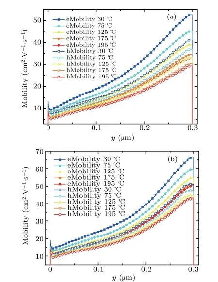
Fig.8.Mobility distributions in(a)GGNMOS mode and(b)GTNMOS mode along path 1 under various ambient temperatures.
3.2. Discussion of GTNMOS
3.2.1. Channel current
Unlike GGNMOS, theVT1of GTNMOS decreases because there exists channel current,IDS, in the period of ESD pulse. TheIDSplays a crucial part in reducing theVT1of GTNMOS mode because theIDSis the main contributor to the increase of the incident currentIpfor the avalanche multiplication at the drain-body junction. The avalanche generation currentIgenis related toIpand the avalanche multiplication factorMby[18]

Before the turning on of BJT, body currentIBody=Igen. TheIpis strengthened byIDS,and a lowerMcan sustain the sameIBody. TheIDSmakesVT1of GTNMOS decrease with respect to that of GGNMOS.Thus,the temperature dependence ofVT1is not simply affected by the avalanche breakdown. As shown in Figs.1(b)and 4,before the first breakdown points,theIDSof the GTNMOS transistor increases with temperature increasing. According to Eq. (2),IDSstrengthensIpand lowersM,which ultimately makesVT1of GTNMOS decrease.
3.2.2. Electrostatic potential
The forward bias of the source-body junction is one of the most essential conditions to trigger the parasitic BJT.The threshold voltage of the source-body junction can be characterized by the electrostatic potential barrier.
Figure 9 shows the distribution of electrostatic potential along path 2 (marked in Fig. 2) before the ESD stress is applied to the drain electrode of DUT.It suggests that the electrostatic potential barrier at the source-body junction decreases when the temperature goes up. The source-body junction can be forward-biased more easily at higher temperatures, which contributes to the turning on of the parasitic BJT at a lowerVT1. Thus, the electrostatic potential barrier of the sourcebody junction decreasing with temperature increasing is one of the factors leading theVT1to decline in the GTNMOS mode.But it is not the major cause in GGNMOS mode compared with the avalanche breakdown behavior.
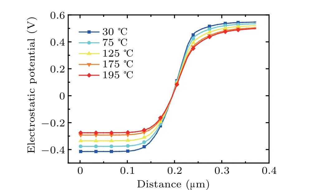
Fig.9. Electrostatic potential distributions in GTNMOS mode along path 2 under various ambient temperatures.
3.2.3. Body resistance
The body resistance,RBody, is defined as the body resistance from the source-body junction to the body electrode.TheRBodyinfluences the body potential near the source-body junction when the body current,IBody,flows through the body region. Previous research has shown that the resistivity of the p-silicon increases with temperature rising in a temperature range from 30°C to 195°C.[19]
The current density distribution in the silicon film can be used to characterizeRBodyindirectly. The total ESD current flows into the DUT through the drain electrode and flows out through the body electrode and the source electrode.Figure 10 shows the total current density distributions of GGNMOS and GTNMOS at five different temperatures. From Fig. 10(b) it can follow that at the same ESD current before GTNMOS is triggered on,the ratio of the body current decreases with temperature increasing. It suggests that the resistance on the path from drain-body junction to body electrode is proportional to temperature. The higher body resistance contributes to higher body potential at the source-body junction, which provides the forward-biasing of the source-body junction and the turning on of the parasitic BJT.
It can be seen in Figs. 10(a) and 10(b) that theIBodyof GGNMOS is larger than that of GTNMOS at each temperature when the parasitic BJT is triggered. TheIBodyfrom the avalanche current in GGNMOS mode is large enough to provide the forward-biasing of the source-body junction, so the major cause to dominate theVT1in GGNMOS mode is the avalanche breakdown threshold but not the positive temperature coefficient ofRBody.
To sum up,the temperature dependence of RBody is another factor to explain the negative temperature coefficient ofVT1in the GTNMOS mode.The body resistance also increases with temperature increasing in the GGNMOS mode as shown in Fig.10(a). Still,it is not the dominant factor when referring to the temperature dependence ofVT1.
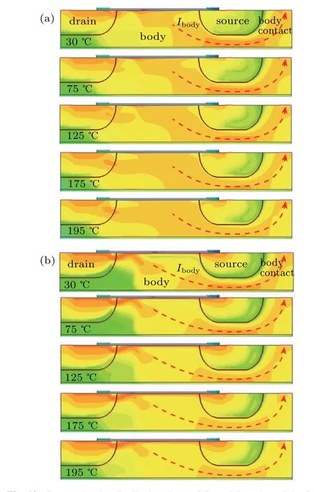
Fig.10. Current density distributions in(a)GGNMOS mode and(b)GTNMOS mode in the silicon film under various ambient temperatures.
4. Conclusions
We have investigated the triggering parameters,VT1,of a PDSOI NMOS device for ESD protecting device operating at elevated temperatures. We conclude the opposite effect thatVT1of GGNMOS increases with temperature increasing and thatVT1of GTNMOS shows reverse variation with temperature. Good agreement is achieved between the TLP measurements,and the TCAD simulated results obtained by the multicurrent pulse simulation method. More analyses of the temperature dependence ofVT1in the two modes are conducted by using TCAD simulation outputs. In the GGNMOS mode,the variation ofVT1with temperature is governed by the avalanche breakdown of the drain-body junction while the temperature dependence ofVT1in the GTNMOS mode is dominated by the channel current and triggering of the parasitic BJT.This study offers a useful insight into and the information about obtaining the safe margin of the triggering parameters of PDSOI NMOS devices operating in a high-temperature ESD protection environment,and also presents the way of weakening the temperature effects in the two modes, which can help to design the temperature-insensitive ESD protecting devices.
猜你喜欢
杂志排行

Chinese Physics B的其它文章
- Projective representation of D6 group in twisted bilayer graphene*
- Bilayer twisting as a mean to isolate connected flat bands in a kagome lattice through Wigner crystallization*
- Magnon bands in twisted bilayer honeycomb quantum magnets*
- Faraday rotations,ellipticity,and circular dichroism in magneto-optical spectrum of moir´e superlattices*
- Nonlocal advantage of quantum coherence and entanglement of two spins under intrinsic decoherence*
- Universal quantum control based on parametric modulation in superconducting circuits*