Aging mechanism of GaN-based yellow LEDs with V-pits∗
2019-06-18TianRanZhang张天然FangFang方芳XiaoLanWang王小兰JianLiZhang张建立XiaoMingWu吴小明ShuanPan潘栓JunLinLiu刘军林andFengYiJiang江风益
Tian-Ran Zhang(张天然),Fang Fang(方芳),Xiao-Lan Wang(王小兰),Jian-Li Zhang(张建立),Xiao-Ming Wu(吴小明),Shuan Pan(潘栓),Jun-Lin Liu(刘军林),and Feng-Yi Jiang(江风益)
National Institute of LED on Silicon Substrate,Nanchang University,Nanchang 330096,China
Keywords:GaN-based,yellow LED,aging mechanisms,V-pits
1.Introduction
Over the past few years,GaN-based light-emitting diodes(LEDs)have shown excellent performance and have been applied to solid state lighting(SSL)systems.The color-mixed approach,that is,component red,green,yellow and blue LED are mixed,is an ideal way to generate white light for SSL.[1]However,considering the dif ficult growth and low efficiency of the yellow InGaN-based LED,yellow GaN-based LED is a weak point of color-mixed SSL,which is mainly attributed to high indium content.In order to gain a high efficiency yellow GaN-based LED,great efforts have been made and have made great advances.[2,3]
Nevertheless,with the enhanced performance of yellow GaN-based LED,the reliability of the yellow LED is also the limitation for color-mixed SSL.For reliability studies,the accelerated aging test is the main research method.The aging mechanism of GaN-based blue LED has been investigated,and mainly related to the generation of defects within an active region of the device,[4-6]interdiffusion on metal-semiconductor interface,[7,8]serious deterioration of the package,[9]and electromigration between the metal electrode and semiconductor,[10]etc.
Additionally,it was found that V-shape pits(V-pits)exist in GaN-based LED,which can screen dislocation,and improve the radiative recombination.[11]Besides,V-pits can also make contribution to the reducing reverse leakage current.[12]For hole injection,it was also found that the V-pits give a path for hole injection through sidewall of V-pits and assist holes in being transferred near the n-side of device,realizing more hole distributions over multiple quantum wells(MQWs).[13,14]
However,the aging mechanisms of yellow GaN-based LEDs was barely investigated. Furthermore,considering that V-pits make much contribution to the LED performance whether the V-pits have an effect on the aging process is unknown,it is necessary to investigate the aging mechanism of yellow GaN-based LED and the effect of V-pits on the aging process.
2.Experiments
The samples in this study were grown on patterned Si(111)substrates by metal organic chemical vapor deposition(MOCVD).As shown in Fig.1,the epitaxial structure of the sample was started with an AlN buffer layer,and then a 3.3-µm Si-doped n-GaN layer was grown on it.Subsequently,32-period 5-nm InGaN/2-nm GaN superlattice layers(SLs)were deposited on n-GaN layer.After that,10-nm Si-doped low temperature-GaN was grown before 8-period InGaN/GaN MQW.The p-type layers consisted of p-AlGaN electron barrier layer(EBL),hole injection layer,and heavily doped p-GaN contact layer.After the growth process,the epitaxial wafers were fabricated into vertical LEDs with the size of 1 mm×1 mm.After the chip process,ten LED chips were selected and packaged in an LUXEON structure,whose dominant wavelength(DW)is 561 nm at 35 A/cm2.A high direct current(DC)of 500 mA(50 A/cm2)was applied to each tube at 40°C ambient temperature,thus it was subjected to an electrically stress and lasted 500 h(i.e.,the tube was aged for 500 h).While in the aging process,the light output power(LOP)and current-voltage(I-V)curves of samples were measured at regular intervals by CAS140CT spectrograph and ISP250-211 integrating sphere.In order to clarify the associated failure mechanisms,the temperature-dependent electroluminescence(TDEL)measurements of the device were performed before and after the aging process.

Fig.1.Schematic epitaxial structure of samples in aging test.
3.Results and discussion
The average of normalized LOPs for ten aged chips tested at 35 A/cm2in 500-h aging process is shown in Fig.2(a).It can be seen that after the aging process,the LOP decreases by 4.01%.The inset in Fig.2(a)displays the normalized L-I curves for sample before and after aging.One can find that the LOP decreases slightly.In this paper,the decrease of the LOP is mainly attributed to the increase of Shockley-Rrad-Hall(SRH)recombination and the reduction of the radiative recombination current,which will be discussed below.
For the InGaN-based LED,the carrier recombination mechanism can be inferred by S value according to L∝IS.When the SRH recombination dominates,S equals 2.While the radiative recombination dominates,S value is 1.And S value less than 1 means carrier leakage by over flowing quantum wells(QWs).[15]Figure 2(b)shows the S values calculated by L-I curves before and after the aging process.With the aging time increasing,the S value rises at each test current density.Figure2(b)can be divided into the upper and lower region by the S=1 line.For the upper region,S value is greater than 1 and shifts from 1.23 to 1.30 at 0.35 A/cm2,which is closer to 2.This phenomenon indicates that the non-radiative recombination increases,which is attributed to the increase of SRH recombination.For the lower region,S value is less than 1,which is mainly due to the carrier over flowing QWs.Similarly,at the current density of 10 A/cm2,S value increases from 0.83 to 0.89 after aging and gets closer to 1.This indicates that the number of over flowing carriers decreases,which is also attributed to the increase of the SRH recombination and consumes more carriers.
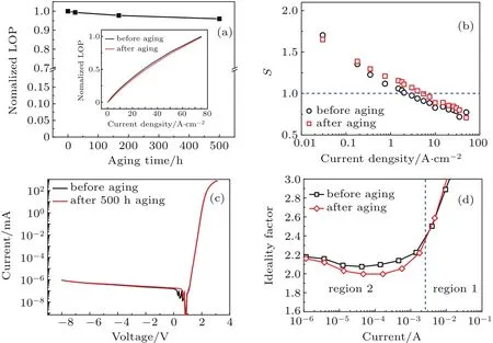
Fig.2.(a)Average LOP of analyzed sample tested at 35 A/cm2in 500-h aging process.Inset shows L-I curves for sample before and after aging.(b)S value versus current density before and after aging process.(c)The I-V characteristic of sample before and after aging.(d)Ideality factors versus current density for the sample before and after aging.
The current-voltage(I-V)curves for the sample before and after a 500 h aging process are plotted in Fig.2(c),and there is no signi ficant increase in leakage current after aging,which means that the samples have stable electrical property.It is known that the ideality factor(n)can be used to analyze the recombination mechanism of the diode.An ideality factor close to 1 means that the direct band-to-band recombination is dominated.A value close to 2 is attributed to the SRH recom-bination via defect level.And the high ideality factor(n≫2)means defect-assisted tunneling phenomenon.[16-18]Consequently,the ideality factors for samples are calculated according to I-V curves and the results are shown in Fig.2(d)which can be divided into two regions.In region 1,one can find that the ideality factor increases rapidly with the current density increasing,which is attributed to the series resistance.[18]In region 2,both the ideality factor for sample before and after aging areboth greaterthan 2.However,theidealityfactorafter the aging process is getting closer to 2,which indicates that the recombination mechanism changes after aging.Before aging,the defect-assisted tunneling dominates.While after aging,the SRH recombination via defect dominates instead.That is to say,more SRH recombination centers are generated after aging,which is consistent with the conclusion obtained by the change of the S value.
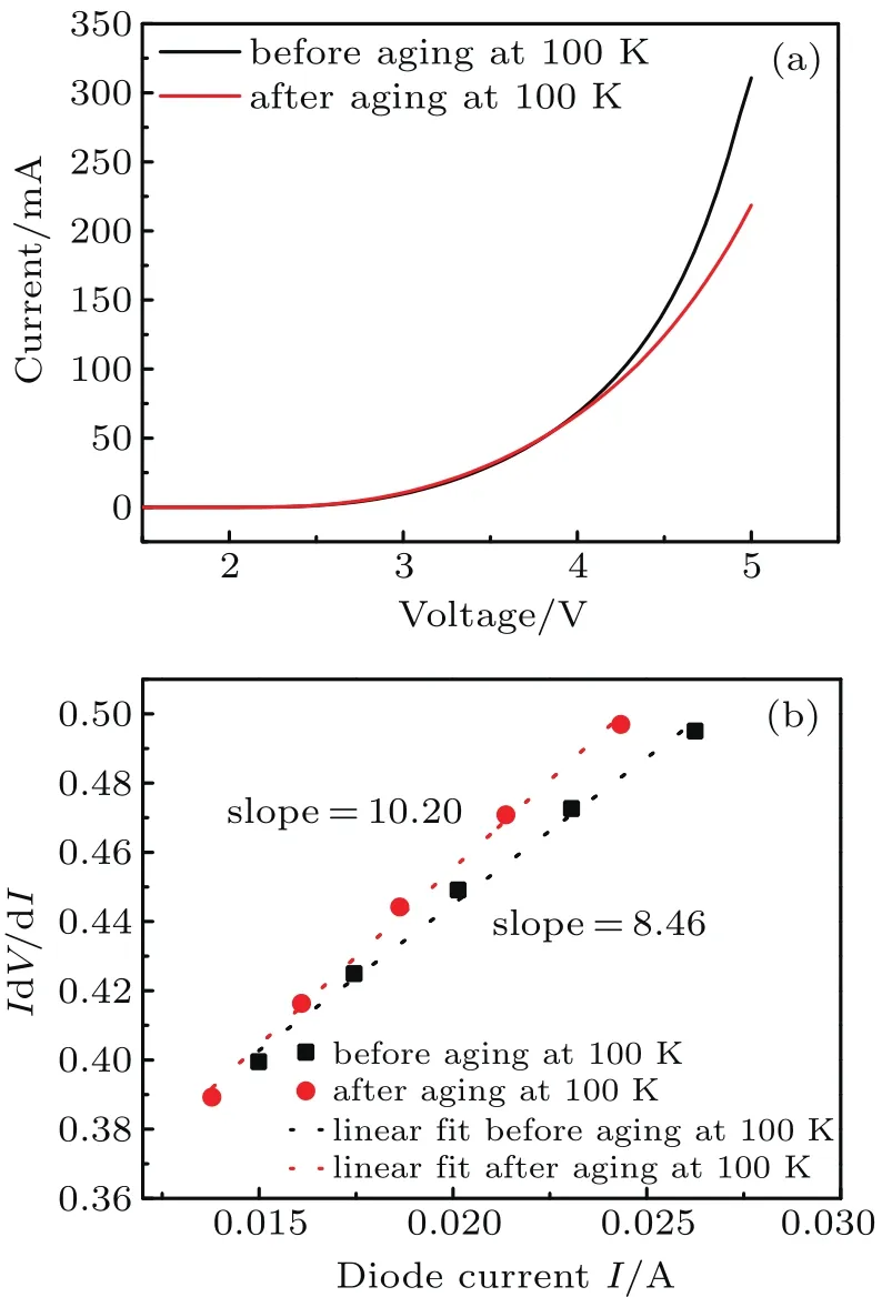
Fig.3.(a)The I-V curve of sample before and after 500-h aging at 100 K.(b)Calculated series resistance via slope of a(IdV/dI)-I for sample at 100 K before and after aging.
Then,the photoelectric properties of the sample before and after aging are tested at 100 K and the I-V curves are shown in Fig.3(a).It can be seen clearly that the operating voltage of the sample after aging is higher than before aging at the same current.The increase of voltage at high current indicates the increase of resistance after aging.Thus,the series resistances for samples are calculated by I-V curves according to Ref.[19].The slope of(IdV/dI)versus I is identi fied to calculate the series resistance of LED.As shown in Fig.3(b),the series resistance increases from 8.46 Ω to 10.20 Ω at 100 K.The increase of the series resistance may be due to the reversible dissociation of Mg-H complexes on the p-type side of the device,which is attributed to the self-heating effect during aging.[20]The Mg-H complexes are dissociated in the initial stage of the aging,then the dissociated H reacts with MgGa,thus forming new Mg-H complexes or metastable Mg-H2complexes.Thereby the effective doping of the p-type layer decreases,which is responsible for the increase of series resistance.These complexes can also act as impurity levels respectively at about 0.12 eV and 0.22 eV above the valence band edge.Additionally,these impurity levels can consume partial carriers.[21]
The EL spectra tested at 100 K are plotted on a logarithmic scale as shown in Figs.4(a)and 4(b).The sample before and after aging has three peaks which are marked as P1,P2,and P3.The cross sectional TEM image of the V-pits of analyzed sample is shown in Fig.4(c),which displays the V-pit tip originating from SLs and embedded in MQWs.Additionally,the EBL and MQWs on c-plane are 3-5 times thicker than those on sidewall of V-pits.Also,in view of the existence of the V-pits in LED epitaxial structure,the transport path of holes via V-pits will change after aging.As shown in Fig.4(d),there are five directions for holes’injection:(I1)injection into c-plane QWs through the flat c-plane region,(I2)injection into c-plane QWs via the sidewall of V-pits,(I3)injection into QWs of sidewall of V-pits and partaking in radiative recombination,(I4)non-radiatively recombination at dislocations in V-pits,(I5)injection through the sidewall of the V-pits and recombination in SLs radiatively.[22,23]According to the transport path of holes,P1is the main emission peak of the c-plane MQW,whose wavelength is around 550 nm at typical 35 A/cm2and shows a blue-shift with current density increasing.As for the shortwavelength emission,it can be seen clearly that P2appears at about 500 nm(35 A/cm2)and P3with a shorter wavelength for about 445 nm(35 A/cm2).P2is different from P1and P3,and is considered as the broadened emission of the sidewall MQWs in the V-pits.[17,20]In addition,P3is attributed to the emission from the InGaN/GaN SLs sandwiched between the n-type GaN and MQW active layer.[18]So,as can be seen in EL spectra,the emission of P2is attributed to the I3direction of holes injection.P3comes from SLs.Due to the thickness of the top MQWs and multi quantum barriers(MQBs),it is hard for holes to be injected along the c-axis direction,while they can be more easily injected through the sidewall of V-pits along the direction I5bypassing the top yellow MQWs.
It is noteworthy that although the sample has three peaks both before and after aging,the EL intensities of P2and P3for the sample after aging are much higher than those before aging,especially for P3.This indicates that the number of holes injected into SLs for sample after aging is more than before ag-ing, namely after aging, less holes are injected into the MQWs.Additionally,after aging,P2and P3start to appear earlier with the increase of current density.It can be seen in Fig.4(b)that after aging the P2and P3start to appear when the current density is 0.18 A/cm2,while before aging they start to appear at 0.75 A/cm2as indicated in Fig.4(a).The phenomenon indicates that after aging the holes are more easily transferred into the SLs.

Fig.4.EL spectra of samples before(a)and after(b)aging as a function of injection current at 100 K.(c)Cross sectional TEM image of the V-pits.(d)Image showing different ways of injecting holes via V-pits.
Because the EBL in the c-plane region is 3-5 times thicker than on the sidewall of V-pits.The quantity of Mg-H complex in the c-plane region is more than on the sidewall of V-pits.After aging,the resistance increases more in the cplane region than on the sidewall of V-pits,and the voltages applied to these two regions also show a similar change.This increase in voltage can compensate for the energy barrier provided by the sidewall of V-pits,making more holes’current flow via the sidewall of V-pits and injected into the SLs than before aging.[24]In other words,the more holes are injected into the SLs,the less holes are injected into the QWs,which can reduce the current participated in radiative recombination in MQWs at 100 K,further lead LOP to decrease.Note that here,the holes’injection mechanism for the sample after aging is changed at cryogenic temperature,and this mechanism may change for devices at room temperature,even reduce the LOP,which needs further investigating in the future.
4.Conclusions
In this paper,the aging mechanism of yellow GaN-based LEDs with V-pits on Si substrates is investigated.It is found experimentally that the decay of LOP is mainly attributed to the increase of SRH recombination.Furthermore,the aging process causes the degradation in the p-side layer,and induces the voltage applied to the c-plane region and the side wall of V-pits to change.Based on the EL spectrum at 100 K,this voltage change causes more holes to be injected into SLs via sidewall of V-pits,which means that less current participates in radiation recombination in MQWs after aging than before aging.This mechanism may also work for devices at room temperature,which needs further investigation in the future.
猜你喜欢
杂志排行

Chinese Physics B的其它文章
- Topological superconductivity in a Bi2Te3/NbSe2heterostructure:A review∗
- The universal characteristic water content of aqueous solutions∗
- Neutral excitation and bulk gap of fractional quantum Hall liquids in disk geometry∗
- Direct deposition of graphene nanowalls on ceramic powders for the fabrication of a ceramic matrix composite∗
- Hard carbons derived from pine nut shells as anode materials for Na-ion batteries∗
- Crystal structures and sign reversal Hall resistivities in iron-based superconductors Lix(C3H10N2)0.32FeSe(0.15<x<0.4)∗