Photoinduced phase transitions in two-dimensional charge-density-wave1T-TaS2*
2019-05-11WenWen文雯ChunheDang党春鹤andLimingXie谢黎明
WenWen(文雯),Chunhe Dang(党春鹤),and Liming Xie(谢黎明),†
1CASKey Laboratory ofStandardization and MeasurementforNanotechnology,CASCenterforExcellence in Nanoscience,NationalCenterforNanoscience and Technology,Beijing 100190,China 2University ofChinese Academy ofSciences,Beijing 100049,China
(Received 23 February 2019;revisedmanuscript received 18March 2019;published online8 April2019)
Keywords:charge density wave,phase transition,1T-TaS2,photodetection
1.Introduction to structure and charge-density waves in 1T-TaS2
Low-dimensional strongly correlated electron systems arise from the couplings between charge,spin,and lattice.They exhibit rich phase transitions,such as superconductivity,ferromagnetism,and charge-density wave(CDW)ordering.[1–4]CDW states comprise a periodic charge-density modulation and a periodic lattice distortion,which originate from the electron–phonon interactions and/or Ferm i surface nesting.[5–9]Due to the collectivemode of charge density,a f initeelectronic bandgap openswith the forming of the CDW phase.[10–12]
The theory of the electron–phonon interaction of the CDW system was f irst suggested by Peierls in 1955.[6]For a one-dimensional(1D)metal chain at temperature T=0 K withoutconsidering the electron–electron orelectron–phonon interactions,the ground state is schematically presented in Fig.1(a).The atom ic chain possesses a lattice constant of a and the electronic states are f illed up to the Ferm i surface EF.A fter taking electron–phonon interaction into consideration,the lattice distortionwith a period ofλismore energetically favorable.The periodλis related to the Fermiwave vector kFbyλ=π/kF.The lattice distortion opens a f inite energy gap 2Δat the Ferm i level(Fig.1(b)),thus turning the metallic phase into insulating CDW phase.Compared to the metallic phasewith constantcharge density ofρ0,CDW states exhibitaperiodic collectivemodewithmodulated chargedensity,which can be expressed as[6]

whereρ1andφare the amplitude and phase of periodically modulated electron density,respectively,and r is thedisplacement.
1T-TaS2,with a plane of Ta atoms sandw iched between two layersof Satoms in an octahedral lattice,exhibits temperature-dependentCDW orderings.Ata temperature below 550 K,the incommensurate(IC)CDW phase formswith slightly distorted lattices.As the temperature is lower than 350K,nearly commensurate(NC)CDW formswith insulating commensuratedomainsand conductivedomainwalls.Further lowering the temperature down to 180 K,insulating commensurate CDW(CCDW)phaseoccurs(Fig.2(a)).In the CCDW phase,the lattice distortion is characterized by asuperlatticeof David-starscomprised of12 Taatomsaround a 13th Ta atom(Fig.2(b)).
The resistance of 1T-TaS2changes in the differentCDW states.For bulk crystal,two abrupt changes of resistance can be observed at temperatures of 180–220 K and 350–360 K,corresponding to CCDW–NCCDW and NCCDW–
The fertilephase transitionsin 1T-TaS2havebeen investigated by versatile tools.For instance,the distribution of electronic density in real space,the conf iguration and electronic structure of domain walls,and the manipulation of CDW phases have been extensively studied by scanning tunneling m icroscopy.[15–19]The ultrafast photoem ission spectroscopy has been introduced to monitor the dynamics of electronic structure in the phase transition process.[20–24]The ultrafast diffraction technique has been developed to reveal the lattice dynamicsof CDW phase transition process.[25–27]ICCDW phase transitions,respectively(Fig.2(c)).[13]As the thickness of 1T-TaS2decreases,the NC–C phase transition disappears(Fig.2(d))as the thickness is less than 9 nm and 3 nm,respectively.The thickness-dependent phase transition behaviorwasexplained asslow kineticsofphase transition.[14]Itwas further found that the NC-to-C phase transition process disappeared athigh cooling rate.[14]Zhang and hiscolleagues attributed the thicknessdependence to the periodicity for sustaining long-range order,dielectric environment,and surface impurities.[13]
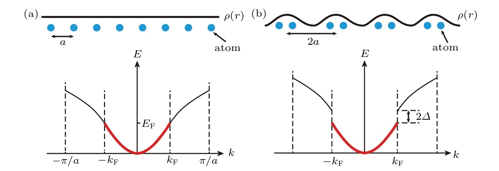
Fig.1.Schematic illustration of one-dimensionalperiodicmetallic latticeand Peierls distorted insulating lattice.(a)Withoutelectron–phonon interaction,the latticewith a period of a exhibits a constant charge density and f illed electron states up to Ferm i level.(b)Considering the electron–phonon interaction,the Peierls distortion results in the periodicallymodulated charge density and an energy gap at the Ferm i level.Reproduced from Ref.[6]with perm ission.Copyright1988,American PhysicalSociety.

Fig.2.CDW phase in 1T-TaS2 at different temperatures.(a)The CCDW,NCCDW,and ICCDW phases at different temperatures.(b)Crystal structure of 1T-TaS2 with David-star clusters consisting of 13 Ta atoms.(c)Temperature-dependent resistance of bulk 1T-TaS2.(d)Temperature-dependent resistanceof 1T-TaS2 with thicknessof 6 nm.As the thicknessof 1T-TaS2 decreases,the phase transition from NC to IC phase isunresolvableow ing to the slow kinetics.(c)and(d)were reproduced from Ref.[13].Copyright2015,Springer Nature.
Additionally,Raman spectroscopy is sensitive to the collective lattice vibration,which has been demonstrated as an effective approach for measuring the CDW phase transition.[28–32]Compared to the undistorted metallic lattice,the commensurate domains consisting ofsuperlattice exhibit fold-back acoustic and optical modes with Raman frequency of 50–100 cm-1and 230–400 cm-1,respectively.[28]With the transition from CCDW–NCCDW phase,an abrupt red-shift of Raman peakswas observed.[30]In striking contrast to theelectricalmeasurements,the Raman spectroscopy demonstrated that fold-back acoustic and optical modesare preserved inmonolayer1T-TaS2.This resultpossibly suggests thatCDW phaseordercan bestableatmonolayer 1T-TaS2.
Further electricalmeasurements have been conducted to investigate the correlation between the CDW states and electron transport properties.The signif icant change of electrical conductivity during the phase-transition process promises the characterization of dynamics of CDW states through electricalsignals.Forexample,the low-frequency noiseofelectrical devices can be employed to understand the sliding of CDW domains.[33]Electricaloscillators,consisting ofa1T-TaS2device in serialwith a load resistor,can beharnessed to study the dynam icsofmultistate phase transitions.[34,35]
Ow ing to the striking differences in electrical conductivity for various CDW states,themanipulation of CDW phases can be exploited to developmultifunctional devices.For example,Iwasaand his colleagues discovered amem ristive NCto-C phase sw itching behavior,arising from an extremely slow phase transition process with reduced thickness of 1TTaS2.[14,36]This work provided a proof-of-principle demonstration of nonvolatilememory devices based on the sluggish CDW phase transition of nano-thick 1T-TaS2.The NC-to-IC phase transition ismore attractive for the practical device implementations because itoccurs at room temperature and can be triggered by optical pulses or electrical current.By collecting a 1T-TaS2in serialwith a load resistor,electrical oscillation can be achieved by revisable sw itching between NC and IC phases.[34]Compared to the conventional ring oscillators,the CDW oscillators based on phase transition possess much simplif ied electrical circuits.Therefore,multiple CDW phase transition of1T-TaS2,togetherwith itselectrical/optical manipulability and low dimensionality,perm its 1T-TaS2as a platform for fabrication ofmultifunctionalphase-transition devices.
In addition to thermodynam ic ground states at different temperatures,light pulses can drive the CDW phase transition and create fertile out-of-equilibrium intermediate states.For the phase transition triggered by light pulses,two effects w ill contribute to the collapse of highly ordered commensurate domains.First,the photo-injected electrons can f ill the Mott–Hubbard bands,yielding mobile carriers to screen the Coulomb interaction between Ta atoms.With the collapse of Ta clustersand strongly correlated electronic states,highly conductivemetalstates can nucleate and grow.Second,highf luence photon injection can give rise to Joule heating effect,which w ill increase the local temperature of the sample.Because the local temperature ishigher than the phase-transition temperature,melting of CDW domain occurs.Therefore,special light–matter interactions can be observed in the CDW phaseswith strongly correlated electron system.
In this review,we have summarized the recent progress on the photoinduced CDW phase transitions in 1T-TaS2,as well as the potential applications.First,the dynam ics of optical pulse induced CDW phase transition in 1T-TaS2is introduced.Second,the out-of-equilibrium intermediate/hidden states,which can only beaccessibleby applying externalstimuli,such as ultrafast laser pulses and electric f ield,are introduced.Third,potential applications of 1T-TaS2as photodetectorsare introduced.Finally,wehave prospected challenges and potentialapplicationsbased on photoinduced CDW phase transitions.
2.Ultrafast optical pulse induced CDW phase transitions in 1T-TaS2
Phase-transition dynam ics in 1T-TaS2have been extensively studied by ultrafast optical stimulation.Fem tosecond electron diffraction was used as a powerful tool to investigate the dynamics of crystal lattice during optical pulse induced phase transition.In the experiments,fem tosecond laser pulseswere employed to initiate the phase transition of 1TTaS2from a highly ordered phase to a low ly ordered phase and an ultrafast electron beam was used to probe the lattice dynam ics.[25,27]The dynam icmelting,sw itching,and recovery processes have been extensively studied with this technique.In addition to electron diffraction,time-resolved xray photoelectron spectroscopy is another effective approach for investigating theevolution of CDW ordering underoptical excitation.These ultrafastmeasurements employed different probes,such as x-ray and electron beams,to collect signals characterizing the structural dynamics,while using fem tosecond lightas a pump source to trigger the CDW phase transition.
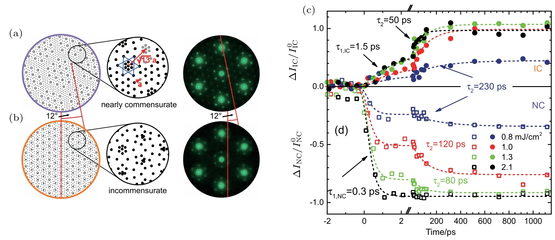
Fig.3.Theultrafastopticalpulse induced NC-to-IC phase transition of 1T-TaS2 monitored by ultrafastelectron diffraction.Realand reciprocal space representation of(a)NCCDW phase,and(b)ICCDW phase.Compared to the ICCDW with slight lattice distortion,the NCCDW phase consists of commensurate supercells,which exhibits~12°-rotated high-order diffraction peaks.(c)The evolution of NC and IC intensities under differentexcitation densities.This f igurewas reproduced from Ref.[25]with perm ission.Copyright2016,American Physical Society.
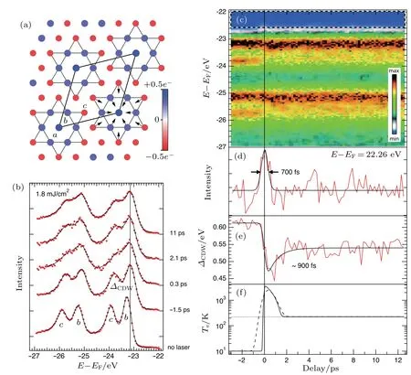
Fig.4.The ultrafast optical pulse induced CDW phase transition monitored by time-resolved x-ray photoem ission spectroscopy(TR-XPS).(a)Scheme of CCDW 1T-TaS2 consisting of David-star clusters with inequivalent a,b,and c Ta atoms.(b)Ta 4f XPS spectra at different delay times.The color represents the electron density,which increases towards the center Ta atom.The Ta 4f photoemission is split into two peaks,corresponding to sites b and c,separated by 2Δ(i.e.,ΔCDW).(c)Two-dimensional false colormap of Ta 4f photoem ission spectra at different delays.(d)Time-resolved photoem ission intensity at E-E F=-22.26 eV.(e)Dependenceof 2ΔCDW on the delay time.(f)Delay-time-dependent electron temperature T e.This f igurewas reproduced from Ref.[23]with perm ission.Copyright2010,American Physical Society.
At room temperature,the ground state of 1T-TaS2is the NCCDW phase,which possesses commensurate CDW domains ref lected by~12°-rotated diffraction peaks in electron diffraction patterns(Fig.3(a)).Under the light excitation exceeding a threshold,themelting of CDW domains occurs,ref lected by the suppressed diffraction of NC superlattice and enhanced diffraction of IC phase(Fig.3(b)).By extracting the timeevolution of NC and IC intensities,a two-stage phase transition process has been discovered.In the f irst stage,the drop of NC diffraction intensity and the rise of IC intensity occurwithin 0.3 psand 1.5 ps,respectively,which is independent of the pump f luence.In the second stage,the drop/rise of NC/IC intensity keeps ranging from 50 ps to 230 ps depending on theexcitation power.The two-stepmelting of NC and buildup of IC phaseareattributed to thenucleation ofnew phase followed by the domain grow th.
The pump-f luence-independentnucleation rate indicates the absence of a nucleation barrier at the f irst stage.The dynamics of phase transition was proposed by Haupt et al.by combining the experimental results and theoretical calculations.They found that the changes in ionic potential,arising from the fem tosecond laserexcitation,give rise to thecoherent atom ic motion in commensurate domains towards the undistortedmetallic domain walls.At the time scale of~1 ps,the energy dissipation to lattice results in the rise of lattice temperature beyond the critical temperature of NC-to-IC phase transition.Further grow th of IC phase requiresmuch atomic displacementwith the transformation of the previously commensurate domains.Overall,complete transformation of NC to IC phase occurswithin the time of~50 psand can be explained by thenucleation and grow thmechanism.
In addition to the ultrafast electron diffraction,timeresolved x-ray photoem ission spectroscopy(TR-XPS)is another effective approach for investigating the dynam ics of CDW phase transition.[23]Thismethod employs three inequivalentTasites(labeled as a,b,and c in Fig.4(a))in CCDW 1TTaS2.In the 13-atom David-star clusters,about0.4 electrons are transferred from outer6Taatoms to innerones.Thecharge transfer in CCDW phase is ref lected by the split Ta 4f peaks in XPS spectra(Fig.4(b)),which can be assigned to b and c sites(peak related to a site isweak to be resolved).The b–c splitting 2Δcan beextracted to characterize theCCDW phase order.Beye etal.performed the TR-XPSwith a free-electron x-ray laser at~156 eV as probe in combination with a synchronized optical pump laserat1.55 eV aspump.Figure 4(b)shows the evolution of XPS spectra at different pump–probe delays.The Ta 4f splitting experiences an obvious reduction within a picosecond followed by partial recovery and formation of a quasi-equilibrium state with a lifetime longer than 10 ps.Figure4(c)shows the false-color TR-XPSspectra.The 2Δdecreases from the original value of 0.62 eV to 0.47 eV,and then recovers to aquasi-equilibrium valueof0.54 eV with a time constantof~900 fs.The lattice temperaturewas calculated and thequasi-equilibrium temperaturewas226K.The ultrafastTR-XPS can beexplained by two processes.The f irst process is the transient collapse of charge order by f illing of the Mott–Hubbard band and collapse of the Mott phase,ref lected by the transientheating of electrons.Then,cooling of electronsoccurs through transferring energy of crystal lattice,yielding aquasi-equilibrium state.
3.Hidden CDW phases in 1T-TaS2
A single ultrafast laser pulse can also trigger the formation of hidden stateswith well-organized CDW domains and undistorted metallic domain walls in 1T-TaS2.Stojchevska et al.reported the generation of a metallic hidden states at 1.5 K by applying a 35-fs laser pulse.[37]At temperaturesbelow 180 K,1T-TaS2exhibitsan insulating CCDW state.A fter applying a 35-fs laser pulse exceeding the power threshold,an abruptdrop of resistancewasobserved,suggesting a phase transition from CCDW to ahidden state(Fig.5(a)).[38]A constant resistance hasbeen observed up to temperatureof 60 K.Upon 100 K,the resistance is close to thatof the C state.The hidden statescan beerased by a train of10450-pspulses.
A mechanism of the hidden-state formation is proposed by combining the experimental results and theoretical considerations.In CCDW states,the electronic states are contributed by the Ta d bands.The 12 electrons contributed by the 12 Ta atoms form occupied states,while the 13th electron is localized at the center Ta atom.The empty upper Hubbard bandsand f illed loweronesare generated by the 13th electron and open an energy gap to sustain the insulating CCDW state(Fig.5(b)).A fter an ultrafast laser pulse,the injected electrons and holes f ill the upper and lower Hubbard bands after ultrafast intraband thermalization,thus inducing themelting of C clusters.The organization of insulating CCDW domains and domain walls after the partial breakdown of the Davidstar clusters promote the formation of a long-range ordered hidden state.Note that thismodel is consistentwith experimental results and theoretical understandings.However,direct characterization of the C domain structure in this hidden state is required to provide deep understandings in its formationmechanism and physicalproperties.
The electric f ield can also be harnessed to trigger phase transitions in 1T-TaS2.[39–42]Vaskivskyi et al.reported the buildup of the conductive hidden states by pulsed current injection.[39]The currentpulse passed through the sample can turn the insulating CCDW phase to ametallic hidden state with a high sw itching speed(30 ps),which provided a proofof-principle demonstration of CDW phase transition for nonvolatilememory.
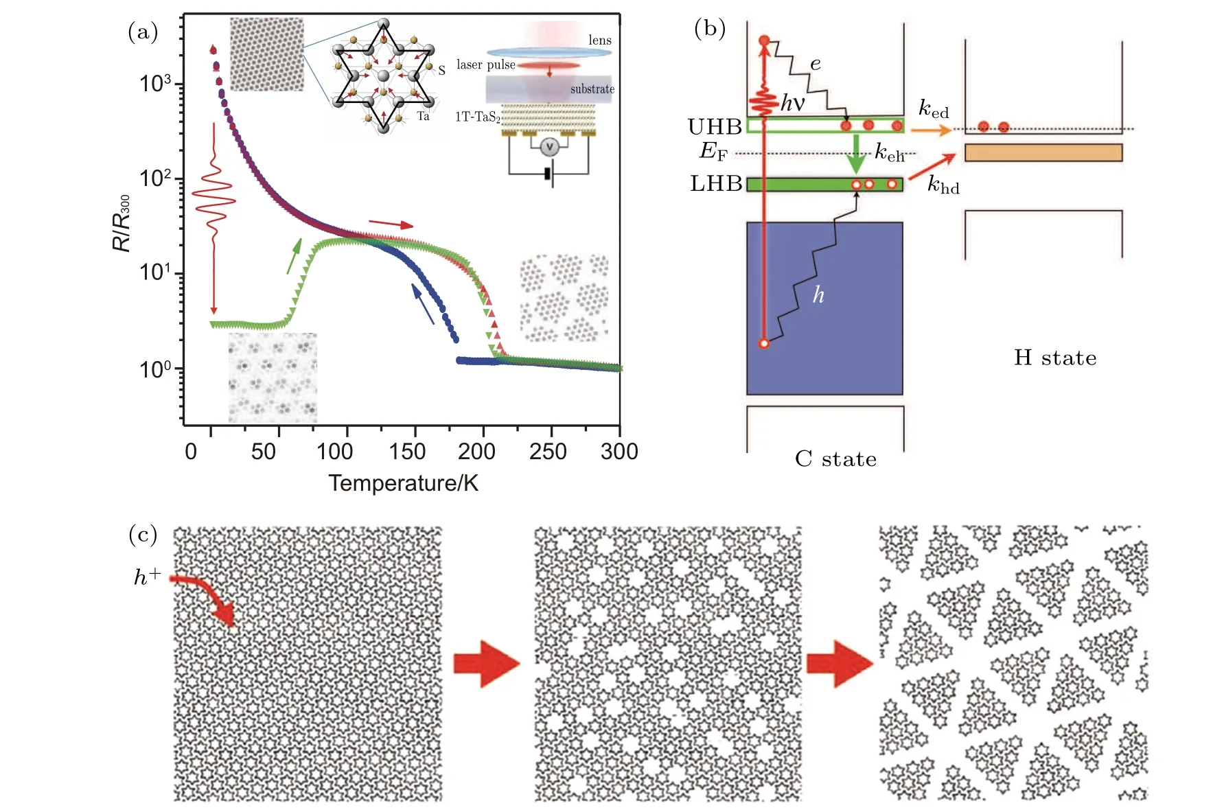
Fig.5.The buildup of a hidden state by applying a35-fs laser pulse.(a)An abruptdrop of electrical resistance can be observed after a single 35-fs laser pulse,which can be attributed to the formation of a hidden state.(b)Representation of energy diagram presents the buildup of the hidden states.(c)The phase diagram after a35-fs laser pulse.(a)was reproduced from Ref.[38]with perm ission.(b)and(c)were reproduced from Ref.[37]with permission.Copyright2014,AAAS.
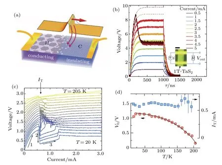
Fig.6.CDW phase transition driven by electricalpulse.(a)The phase transition can be driven by electricalpulse.Asan electricalpulse travels through thesample,themelting ofC phaseoccurs togeneratehighly conductivehidden states.(b)Temporalresponseof1T-TaS2 by applyingacurrentpulse.(c)The pulsed V–I characteristic atdifferent temperatures.(d)The temperature-dependent V0 and I T.V0 is the voltage at I=0mA and I T is the threshold current for the phase transition.This f igurewas reproduced from Ref.[39]with perm ission.Copyright2016,Springer Nature.
During the currentpulse triggered phase transition,there are several characteristics.First,with the increase of current density of electrical pulse,an abrupt drop of electrical resistanceoccurs in 1T-TaS2,indicating the phase transition from a Mottinsulator to ahighly conductivemetallic state(Fig.6(b)).Second,the CDW phase sw itching is strongly dependent on the pulse duration time.For pulseswith duration time higher than 0.1 ps,phase sw itching is incomplete or cannot occur.Themeasurablephasesw itching speed can reach30 ps.Third,electrical-pulse-driven phase transition presents a signif icant dependenceon temperature(Figs.6(c)and 6(d)).Theobvious sw itching only occurswith temperature ranging from 10 K to 55K.In the rangeof55K to 165K,unstablevoltage response wasobserved above a threshold current.Based on these facts,Vaskivskyi etal.proposed amechanism based on the formation of a hidden state sim ilar to the fem tosecond laser pulse excitation.[39]The injected charges can cause the partial collapse of the David-star clusters and the establishment of organized David-star domains separated by conductive domain walls.
Optical pulses and electric f ield can drive CDW phase transitions in 1T-TaS2.However,themechanism for the phase transition triggered by electric f ield and optical pulses is still under debate.Recently,Shao etal.studied the electron and hole doping of 1T-TaS2by using density-functional-theory(DFT)calculations.[43]They found that the stability of CDW domainscan besuppressed by holedopingwhichweakens the electron density at the center of star-of-David,while the stability of CDW phase isnotsensitive to electron doping.
Compared to the out-of-plane electric f ield,the phasetransition mechanisms driven by optical pulses and in-plane electric f ield aremore complex and still under debate.Two mechanisms are proposed.First,optical excitation and inplane electric f ield can injectmobile holes in 1T-TaS2,which triggers themelting of star-of-David.Second,light irradiation and electrical currentcan generate Joule heat,giving rise to the increase of local temperature over the phase-transition point.Bymeasuring the Stokes and anti-Stokes Raman spectra of 1T-TaS2during the phase-transition process driven by in-planeelectric f ield,[44]we found that the local temperatures range from 295 K to 320 K,which excludes the Joule heating mechanism in thiscase.
4.Bolometers based on CDW phase transitions in 1T-TaS2
The CDW phase sw itching can be driven by light irradiation in 1T-TaS2,thus leading to their practical application as photodetectors.In contrast from semiconductorswith a f inite bandgap and thus the photodetectorswith a narrow spectral response,the photodetection based on phase transition possess a broadband response.Due to itsmetallic nature,1T-TaS2exhibitsbroadband lightabsorptionwith wavelength ranging from severalhundreds of nanometers to 100m icrometers(Fig.7(a)).
Before discussing the photodetection applications,we brief ly summarize the synthesismethods for high-quality 1TTaS2two-dimensional(2D)nanof lakes,which isimportant for scalable construction of high-performance devices.Mechanical exfoliated nanof lakes exhibit high crystallinity,but their practical device applications are limited by the low fabrication eff iciency.The chem icalvapor deposition(CVD)method has been employed to fabricate 1T-TaS2.Liu and his colleaguesdemonstrated that few-layer1T-TaS2can begrown by CVD.[45]Huang etal.synthesized vertically oriented 1T-TaS2with abundant edge sites on nanoporous gold substrates.[46]Xie etal.also demonstrated theCVD grow th of1T-TaS2on h-BN substrate.[30]These resultsprovide thepossibility forscalable fabrication of high-performance devices based on CDW phase transition.
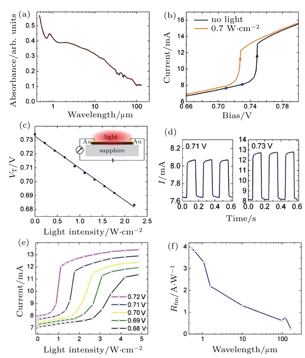
Fig.7.Photodetectors based on the CDW phase transition in 1T-TaS2.(a)Absorption spectrum of 1T-TaS2.(b)The I–V curves of 1T-TaS2 at the dark state and the light illum ination of 0.7W·cm-2.(c)Voltage threshold of NC-to-IC phase transition under different light irradiance.(d)The time response of photodetectors under the light pulse of 5 Hz and 0.7mW·cm-2.(e)The current of device under different light intensities.(f)Spectral responseof photodetector.This f igurewas reproduced from Ref.[47]with perm ission.Copyright2018,AAAS.
At room temperature,the phase transition from NC-to-IC states can be triggered by an ultrafast fem tosecond laser pulsewith a threshold of light intensity.In contrast,Wu etal.demonstrated that the sliding of C domain under the applied electric f ield can bemanipulated by applying lightwithmuch lower power,ref lected by the striking decrease of threshold voltage for the NC-to-IC phase transition(Fig.7(b)).[47]The decreaseof threshold voltage is linearly dependenton the light intensity and the good linearity enables the high-performance light sensing(Fig.7(c)).The abrupt rise and decay of electrical currentwere observed in 1T-TaS2by applying a 5-Hz pulsed light(Fig.7(d)),suggesting the fast temporal response of this photodetector.Wu etal.also studied the evolution of device currentwith the lightintensity atdifferentapplied voltages and the wavelength-dependent responsivity(Figs.7(e)and 7(f)).The highest responsivity can achieve~4 A·W-1for this photodetector.Even under lightwith wavelength of 10μm,the photoresponsivity exceeds 1 A·W-1.Therefore,due to the lack of bandgap for 1T-TaS2at room temperature,it is an ultra-broadband photodetectorwith relatively high response.Since the sliding of CDW domains requiressome lattice distortion,the photodetector exhibits ultrahigh response speed.The rise and decay timeswere recorded as~1.5 ns and 30 ns,respectively.
The ultrathin nature of suspended 2D 1T-TaS2f ilm can haveultralow thermalcapacitanceand then hasextremely high bolometric response.Xie and his colleagues demonstrated highly responsive bolometers based on suspended 1T-TaS2.
The as-grown 1T-TaS2f ilm(around 100 nm thick)exhibits broadband opticalabsorptionwith relatively low transmittance ranging from 20%to 40%(Fig.8(a)).Devices were fabricated by suspending of1T-TaS2and apairofmetalelectrodes(Fig.8(b)).Interestingly,the bolometric effect can contribute to the NC-to-IC phase transition process.At voltages ranging from 0.5 V to 1.4 V,prominentdecreaseof resistancewas observed under applied infrared light(Fig.8(c)).For applied voltageexceeding 1.3V,the resistanceof1T-TaS2experienced a signif icant reduction.When the applied voltage increased to 1.5 V,the change was hard to be observed,caused by the buildup of IC phase under the applied voltage.Therefore,incident photons can heatup the 1T-TaS2and contribute to the NC to IC phase transition through thebolometric effect.
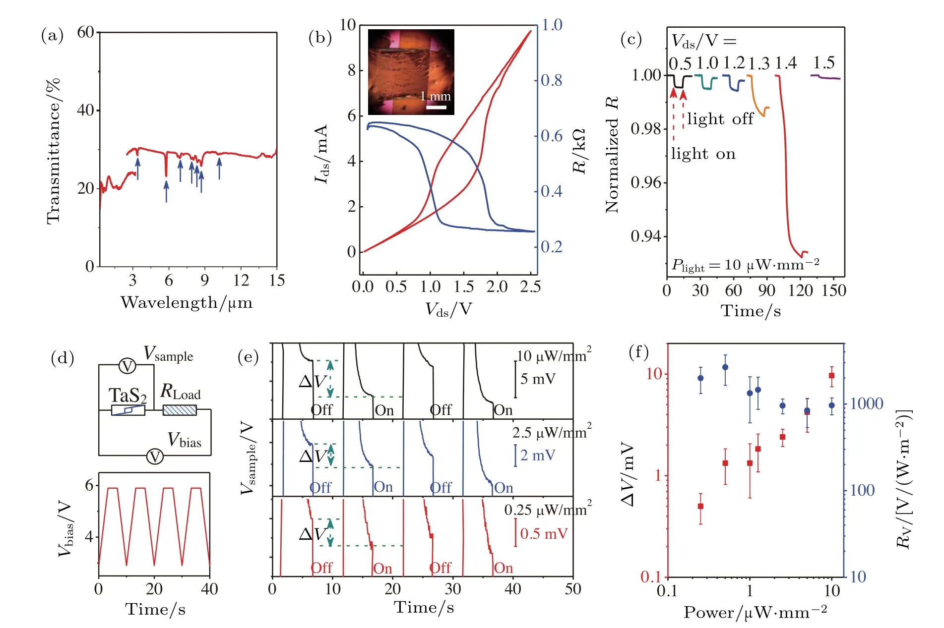
Fig.8.Bolometric performanceof a 1T-TaS2 f ilm.(a)Transm ittance spectrum of 1T-TaS2.(b)Currentand resistance of 1T-TaS2 atdifferent applied voltages.(c)Bolometric resistance response of 1T-TaS2 under IR lightwith irradiance of 10μW·mm-2 atdifferentapplied voltages.(d)Scheme of circuit and the AC electricalwaveform used in the voltage responsivity measurements.(e)Voltage response at different IR irradiance.(f)Derived voltageand responsivity under different illum ination powers.This f igure is reproduced from Ref.[30]with perm ission.Copyright2018,W iley-VCH.
The f igures of merit of 1T-TaS2bolometers were evaluated by constructing a circuit,in which 1T-TaS2was connected in serialwith a load resistor.An alternating current(AC)biaswassupplied to tune the phase transition of1T-TaS2(Fig.8(d)).Under light irradiation,a striking voltage drop of 1T-TaS2was observed due to the decrease of resistance.The responsivity RVis calculated by RV=Vresp/Plight,where Vrespis the voltage difference before and after light irradiation and Plightis the light power.A highest responsivity of 2600 V·W-1·mm2was observed,which ishigher than thatof other bolometers thatare based on strongly correlated phase transition,such as VOXand sem iconducting yttrium barium copperoxide(YBCO).
5.Conclusion and perspectives
Extensive research has been made in CDW phase transitions and their dynamics:from ultrafast melting of CDW domains to the buildup of out-of-equilibrium hidden/intermediate states.The phase transition processes,including themelting of David-star domains and the buildup of new phase,are accompanied with the striking change of electricalconductivity.FertileCDW phasesand theirstriking contrast of electrical conductivity offer an interesting avenue to createmultifunctionaldevices,including photodetectors.Photodetection based on strongly correlated electronic system is strikingly different from conventional semiconductors.Without a bandgap,the CDW-based photodetectors can exhibit broadband photodetection with wavelength ranging from severalhundredsofnanometers to hundredsofmicrometers.The ultrafastmelting,nucleation,and grow th ofCDW ordering offer a core opportunity for the fabrication of ultrafast devices.Although the potentialphotodetection application of 1T-TaS2hasbeen outlined in this review,research on CDW-based photodetectors isstillprelim inary.
First,the mechanism of the photoresponse is still unclear. The photodetectors operated at room temperatures should originate from the NC to IC phase transition.The lattice dynam ics research is carried outby employing fem tosecond optical excitation,in which high f luence of photons are injected into 1T-TaS2within ultra-short time.However,photodetection experimentsare usually performed under continuouswave lightexcitationwith relatively lower f luence,which cannotachieve theultrafastmelting of CDW orderingwithout thehelp of theapplied electric f ield.Therefore,theunderlying mechanisms for theCDW phase transition driven by fem tosecond laser pulse and continuouswave lightare possibly different.In thisrespect,furtherstudiesinto the latticedynamicsunder electric f ield and continuouswave lightexcitation should be carried out to reveal the underlyingmechanism.
Second,the signal-to-noise ratio of the CDW-based photodetectors need to be further improved.Currently,1T-TaS2is stillhighly conductive even at the dark condition,which is due to the conductive domain walls in the NCCDW phase as well as the small CDW gaps.So further research is needed to f ind CDW materialswith amuch lower conductivity in the ground CDW state and amuch higher conductivity in the excited state.We believe that the concept of photodetection based on the CDW phase transition offers new opportunities for creating high-performance photodetectorswith broadband spectralsensitivity,ultrafast response,and an ultrahigh signalto-noise ratio.
杂志排行

Chinese Physics B的其它文章
- Low-tem perature grow th of large-scale,single-crystallinegrapheneon Ir(111)*
- Epitaxial fabrication of two-dimensional TiTe2 monolayer on Au(111)substratew ith Teasbuffer layer*
- Isotopeeffectand Coriolis coup ling effect for the Li+H(D)Cl→LiCl+H(D)reaction*
- V ariationaland diffusion M onte Carlo simulationsof a hydrogen molecular ion in a sphericalbox*
- General way to def ine tunneling time*
- Dynam icsof two levitated nanospheresnonlinearly coup ling with non-M arkovian environment*