Compact 2×2 parabolic multimode interference thermo–optic switches based on fluorinated photopolymer∗
2019-04-13JiHouWang王继厚ChangMingChen陈长鸣KeWeiHu胡珂玮RuCheng程儒ChunXueWang王春雪YunJiYi衣云骥XiaoQiangSun孙小强FeiWang王菲ZhiYongLi李智勇andDaMingZhang张大明
Ji-Hou Wang(王继厚),Chang-Ming Chen(陈长鸣),Ke-Wei Hu(胡珂玮),Ru Cheng(程儒),Chun-Xue Wang(王春雪),Yun-Ji Yi(衣云骥),Xiao-Qiang Sun(孙小强),Fei Wang(王菲),Zhi-Yong Li(李智勇),and Da-Ming Zhang(张大明),†
1State Key Laboratory of Integrated Optoelectronics,College of Electronic Science and Engineering,Jilin University,Changchun 130012,China
2State Key Laboratory of Integrated Optoelectronics,Institute of Electronic Semiconductors,Chinese Academy of Sciences,Beijing 100083,China
1.Introduction
Currently,the highly integrated optical transmission systems are the key components for building broadband optical communication networks.[1–4]Specially,thermo–optic(TO)switching devices are essential parts in photonics integrated circuits which can be applied to reconfigurable optical transmission networks.[5–9]Compared with the fiber-type TO optical switches,the waveguide-type TO switches have captured considerable interest such as functional compact photonic chips with smaller size,lower driving power consumption and faster response.Diversified TO waveguide switching structures have been used in actual optical chips,such as x-junction,[10,11]Mach–Zehnder interference(MZI),[12–14]directional coupling(DC)and multimode interference(MMI)type,[15–19]etc.Compared with the other structural TO waveguide switches,the MMI TO waveguide switches with high integration and lower process tolerance are more suitable to realizing N×N multi-channel integrated switching matrixes for high-quality photonic chips.[20–22]Presently,functional polymers as waveguide materials have been widely adopted for the MMI TO switch with large TO coefficient,tunable refractive index and flexible fabrication process rather than inorganic waveguide materials such as silicon,InP and SOI,etc.[23–27]It can be predicted that the polymer MMI TO waveguide switches may play a significant role in improving the performances of the high-integration photonic circuits for highspeed optical cross-connect system.
In this work,a highly compact 2×2 dual-side parabolic structural MMI TO waveguide switch with larger extinction ratio and lower driving power consumption than the traditional dual-side linear structure of MMI is designed and fabricated based on low-loss fluorinated photopolymer materials.The thermal stability of the waveguide material is analyzed and the optical characteristics of the switching chip are simulated.The structural morphologies of the actual waveguide MMI region and electrode heater are characterized.The actual performances of the entire MMI switches proposed are measured.The types of the MMI TO switches are very suitable for serving as switching matrix of photonic integrated circuits.
2.Experiment
2.1.Waveguide material
To realize the DSPS MMI switches,the low-loss fluorinated photopolymers are synthesized as the core waveguide materials.The functional polymers are composed of fluorinated epoxy resin(FSU-8)and fluorinated epoxy-terminated polycarbonates(FBPA-PC EP).The refractive indices and cross-linking densities of the fluorinated photopolymers can be tuned and controlled by changing the dose of the FSU-8.The waveguide materials are prepared by mixing FSU-8 and FBPA-PC EP with the solvent and a photoinitiator.The molecular structure of FSU-8 and FBPA-PC EP are shown in Fig.1(a).Comparing with the common waveguide materials,C–H bonds replaced by C–F bonds in the photopolymer can reduce the intrinsic optical absorption loss of this waveguide material in the near-infrared wavelength region between 1310 nm and 1550 nm.The near-infrared absorption spectrum of the fluorinated photopolymer film is shown in Fig.1(b).It can be obviously observed that the mixture of FSU-8 and FBPA-PC EP has almost no optical absorption in a range from 400 nm to 2000 nm compared with the commercial photoresist SU-8.
It can be explained that the material absorption loss of SU-8 is mainly due to C–H bond vibration absorption in the near-infrared wavelength region.The model of the vibration absorption can be approximately regarded as simple harmonic motion,and the vibration rate equation is given as
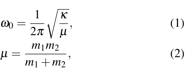
where ω is the vibration base-band of the C–H bond,κ is a chemical constant,µ is the reduced mass of C–H atomic pair,m1and m2are the atomic weight of carbon atom and hydrogen atom,respectively.
The υ-th(υ is quantum number)vibration frequency of diatomic molecule defined υυcan be expressed as

where B is a constant.When the hydrogen atom is replaced with larger relative atomic mass,such as fluorine atom,The molecular mass can be increased and it makes all harmonic frequency reduced.Thus the low loss wave band will have a red shift.So the resonance and coupled vibration absorption of C–F bonds are smaller than those of C–H bonds in near infrared region.[28]The FSU-8 material can significantly reduce the absorption loss.
The refractive index of the cross-linked fluorinated mixture can be tuned from 1.495 to 1.565 at 1550-nm wavelength when the content of FSU-8 is changed from 10 mol%to 75 mol%.The thermal stability of the fluorinated photopolymer is characterized.Tg of this fluorinated polymer,as glass transition temperature,is measured to be 142◦C by differential scanning calorimetry(DSC).The temperature Td for 5%weight loss of the epoxy cross-linked polymer is obtained to be 303◦C by thermo gravity analysis(TGA).Poly(methyl methacrylate)(PMMA)as a mature material for plastic optical fiber(POF)system is synthesized and used as the cladding material.The refractive index of the PMMA is measured to be 1.480 by ellipsometer.The merits of these functional polymer waveguide materials can provide adequate guarantee for realizing the new dual-side parabolic structural MMI switches with high performances.
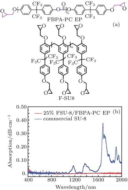
Fig.1.(a)Molecular structure of fluorinated photopolymer(FBPAPC EP and FSU-8);(b)Near-infrared absorption spectrum of FSU-8(25%)/FBPA-PC EP and Commercial SU-8.
2.2.Design of 2×2 parabolic MMI-TO switch
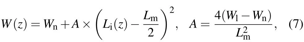
The schematic diagram of the DSPS MMI TO waveguide switch is shown in Fig.2(a).The largest width(Wl)of MMI region connecting to input and output channel is 50µm.The narrowest width(Wn)in the middle of MMI region is 35µm.The length(Lm)of entire MMI region is 1610µm.The electrode heater upon the cladding PMMA is set to be in the center of the MMI region.The width(We)and the length(Le)of the electrode are designed to be 25µm and 400µm,respectively.The width of input and output channel waveguide are both 5µm,and the width of the taper waveguide connecting to the MMI region is enlarged to 10µm for enhancing coupling efficiency.The transitional length for the taper structure is 500µm.The cross-sectional waveguide structure with the electrode is shown in Fig.2(b).The size of the core waveguide is 3µm×5µm.The thickness of SiO2buffer layer on silicon substrate as lower cladding is 5µm and that of the PMMA upper cladding is 2µm.The thickness of the Al electrode is 60 nm.The refractive index of the fluorinated photopolymer,PMMA-GMA and SiO2substrate are 1.526,1.485,and 1.444,respectively.The TO coefficient of the fluorinated photopolymer is−1.85×1−4m−1·K−1.
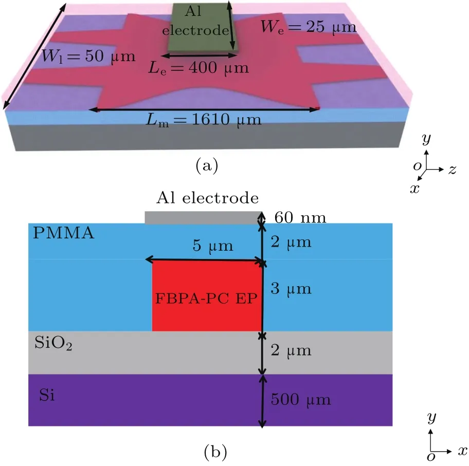
Fig.2.(a)Overall structure of DSPS MMI TO waveguide switch,and(b)cross-sectional waveguide structure with electrode.
2.2.1.Small size of compact MMI region
Compared with the traditional dual-side linear structure of MMI,the DSPS MMI is given in Fig.3(a).It can be found that for the same waveguide material and size,the length Lmof MMI region can be effectively reduced to 38.0%,less than the length of traditional DSLS MMI structure for realizing a similar coupling function.
Based on the self-image principle of MMI,the dispersion relation at any position z of DSPS MMI can be expressed as

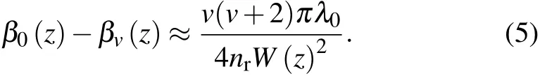
where Kxv(z)and βv(z)are the lateral wavenumber and propagation constant of the mode v at position z,respectively;W(z)is the effective MMI width at the position z of DSPS MMI,and v is a mode number such as 0,1,...,m−1,m,where m is the number of effective modes.and nris the effective index of the traditional MMI region.The propagation constant spacing from the v-th mode to the fundamental one with propagation constants of βv(z)and β (z)can be expressed as

where Wlis the traditional width of traditional MMI region and λ is the signal wavelength.
For the DSPS MMI proposed,the varying width W(z)of the DSPS MMI region can be given as
For the DSLS MMI,the beat length Lπis defined as
where Li(z)is defined as the length of DSPS MMI region,corresponding to different positions;Lmis the total length of the DSPS MMI region;Wlis the largest width of DSPS MMI region connecting to input and output channels,which is also the same as the traditional width of the traditional MMI region;Wnis the narrowest width in the middle of DSPS MMI region at Li=Lm/2.
For the beat length of DSPS MMI region,the formulas are shown as

where nrand ncare the effective in dices of the DSPS MMI region for different widths atW=Wland W=Wn,respectively;Wgdenotes the Goos–Hanchen shift.[16]The factor σ =0 and σ=1 correspond to transverse electric(TE)mode and transverse magnetic(TM)mode,respectively.Because α>1 in the calculating process,the length of the DSPS MMI is shorter than that of the DSLS MMI device as indicated by comparing Eq.(6)with Eq.(8).
According to Eq.(8),it can be obviously indicated that the beat length Lpπof DSPS MMI region is equivalent to Lπ/α,where Lπis the beat length of traditional DSLS MMI in the same condition.As shown in Fig.3(b),it can be depicted that the value of α declines exponentially with Wn/Wlincreasing.Considering the actual fabrication tolerance of electrode heater,the value of Wn/Wlis selected in a range from 0.5 to 1.0.
In the actual designing of DSPS MMI,the radian(C)of the parabolic curve is an important parameter and it is directly related to α.The parameter C plays a key role in reducing the interaction length and scattering loss of MMI region.The relationship between α and C is given in Fig.3(c).From Fig.3(c),it can be found that with α increasing,C becomes large.To control the interaction length and scattering loss effectively,according to the actual experimental parameters,the value of α is optimized to be 1.6.when Wn/Wlis chosen to be 0.7,C is set to be 2.296×10⁻⁵µm−1.So Wnand Wlare determined to be 35µm and 50µm,respectively.In this case,the length of DSPS MMI region is only 62.5%of the length of the traditional DSLS MMI region.
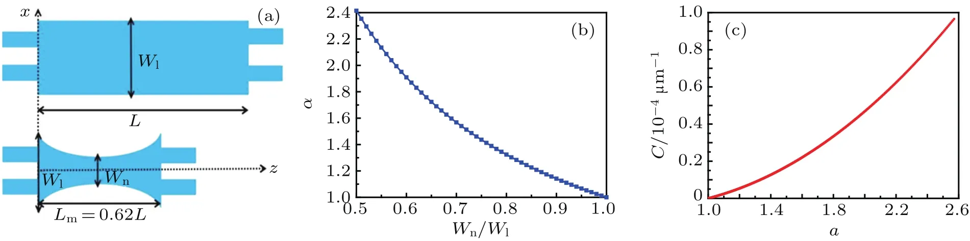
Fig.3.(a)Comparison of length between the traditional DSLS MMI and DSPS MMI;(b)relation between α andWn/Wlof DSPS MMI;(c)relation between α and C of DSPS MMI.
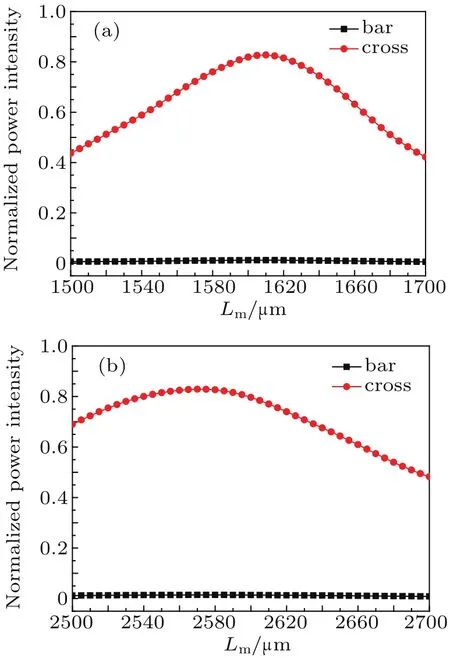
Fig.4.Curves of bar and cross port output power versus Lmfor(a)DSPS MMI device and(b)traditional DSLS MMI device.
When the width Wlis set to be 50µm,the optimized length of DSPS MMI and traditional DSLS MMI region are simulated by the beam propagation method(BPM),and the results are shown in Fig.4.It is demonstrated that as given in Fig.4(a),the optimized length Lmof the DSPS MMI region is 1610µm directly corresponding to the cross state with the output optical normalized power of 83%as shown in Fig.4(b),and the optimized length Lmof DSLS MMI is 2580µm with the output power of 81%in the same state.For the bar states,the output power of DSPS and DSLS MMI approximate to zero.Comparing with the traditional DSLS MMI,the optimized length of DSPS MMI can be effectively shortened by 37.6%in the same case.The wavelength-dependent characteristic of DSPS MMI is analyzed,and the results are shown in Fig.5(a).It can be found that the optical output normalized power of DSPS MMI directly at cross state exhibits good stability in a wavelength range from 1545 nm to 1565 nm in C-band.The relationship between the output power and the width Wlof the DSPS MMI is also calculated in Fig.5(b).It can be observed that when Wlis selected to be 50µm,the output power reaches a maximum value.It is identified that the DSPS MMI can provide small size and high stability for achieving compact photonic integration.
Fig.5.Curves of bar and cross port output power versus(a)wavelength and(b)Wlfor DSPS MMI device.
2.2.2.Low power consumption and large extinction ratio
For the driving power consumption of the TO waveguide switch,the relevant equation is given as
where Leand Weare the length and width of the electrode heater,respectively;H is the thickness of the upper cladding;K is the thermal conductivity and its value is 0.27 W·m−1·K−1for the SiO2cladding,0.2 W·m−1·K−1for the PMMA cladding,and 0.16 W·m−1·K−1for the fluorinated photopolymer;∆T is the temperature change of the electrode heater.As the optimized values,Le,We,and H are set to be 400,25,and 2µm,respectively.The TO coefficient of fluorinated photopolymer,PMMA and SiO2are measured to be−1.85×10⁻⁴K−1and−1.2×10⁻⁴K−1.Based on these designing and experimental data,the optical transmission fields of DSPS MMI switching response from cross to bar state are simulated,and the results are shown in Figs.6(a)and 6(b),respectively.The driving electric power consumption is obtained to be 14 mW.In contrast,the optical transmission fields of DSLS MMI switching response from cross to bar state are analyzed,and the results are displayed in Figs.6(c)and 6(d),respectively.The driving electric power consumption is calculated to be 17.5 mW.It can be demonstrated that the DSPS MMI TO switch,rather than the DSLS MMI TO switch,needs lower driving electric power.Because the effective width of DSPS MMI is narrower than that of DSLS MMI,the optical modes’distribution is more compact.The lower temperature change and shorter interaction length of DSPS MMI is required to drive the power to the bar output port.The relationship between∆T of the electrode and the output power of DSPS TO switch is shown in Fig.7(a)and that of the DSLS TO switch is given in Fig.7(b).It can be found that when∆T for the DSPS MMI and DSLS MMI are 18 K and 21 K,respectively,the bar output port has a maximum output optical power and the cross port has a minimum value.Besides,the effective width of electrode obtained on the DSPS MMI is narrower than that on the DSLS MMI,which means that Wecan be defined as a smaller value.From Eq.(9),the DSPS MMI TO switch can realize lower power consumption than the DSLS MMI TO switch.The optical field distribution of the waveguide and the thermal field distribution of the electrode heater for the DSPS MMI TO waveguide switch are also simulated,and the results are given in Figs.6(e)and 6(f),respectively.About 93.3%of the normalized optical power is confined into the waveguide core,and the driving temperature∆T of the electrode heater is obtained to be 18 K.

Fig.6.(a)Simulations of optical field transmission for (a) DSPS MMI TO waveguide switch with no modulation, (b) DSPS MMI TO waveguide switch with 14-mW driving power TO modulation,(c)traditional DSLS MMI TO waveguide switch with no modulation,(d)traditional DSLS MMI TO waveguide switch with 17.5-mW driving power TO modulation,(e)optical field of input waveguide for DSPS MMI TO waveguide switch,(f)thermal field distribution of MMI region of DSPS MMI TO waveguide switch with 14-mW driving power modulation.

Fig.7.Output power of bar and cross port versus temperature of electrode(∆T)for(a)DSPS MMI TO switch and(b)DSLS MMI TO switch.
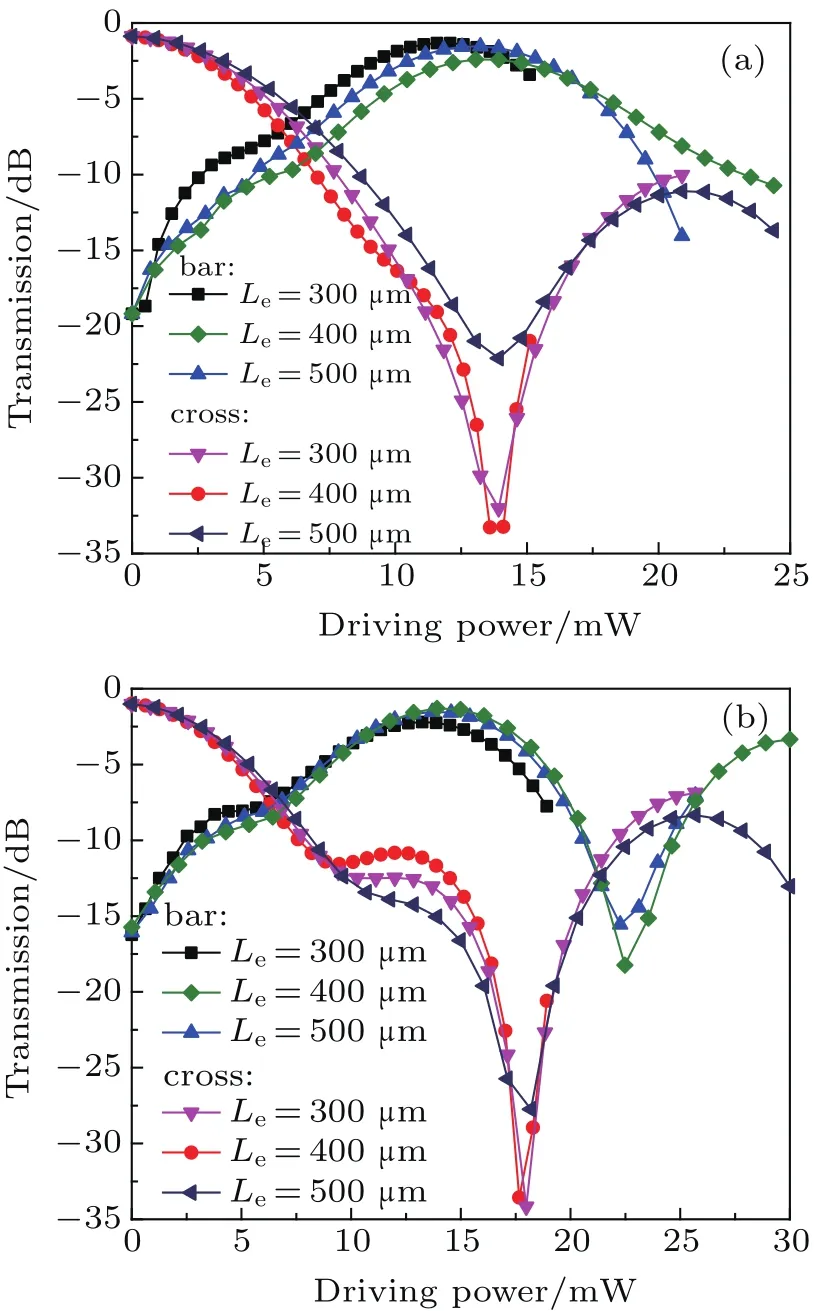
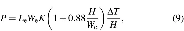
Fig.8.Curves of output power of bar and cross port versus driving power for(a)DSPS MMI TO switch and(b)traditional DSLS MMI TO switch.
The curves for output power of bar and cross port versus driving electric power of DSPS switch and DSLS MMI TO switch are given in Figs.8(a)and 8(b),respectively.The extinction ratio of the DSPS TO switch is 31.2 dB and that of the DSLS TO switch is 27.1 dB.It can be found that the DSPS TO switch,rather than that of the DSLS TO switch,exhibits lager extinction ratio.It can be identified that the DSPS MMI can provide low power consumption and large extinction ratio for realizing high-quality integrated switching matrixes.
2.3.Fabrication and measurement of DSPS MMI TO switch
The DSPS MMI TO waveguide switch is fabricated by direct UV writing technique.The detailed process is shown in Fig.9,similar to those in Refs.[29]and[30]The resistance of the Al electrode heater is measured to be 200 Ω.The profiles of MMI waveguide and electrode heater are given in Figs.10(a)and 10(b)by optical microscope(×200),respectively.It can be seen that the size of the waveguide and electrode can fit well to the parameters designed.
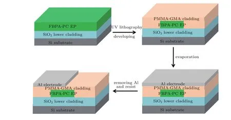
Fig.9.Fabrication process of DSPS MMI TO switch.
The experimental measurement system for the device is shown in Fig.11(a).A tunable laser source(Santec TSL-210)with a wavelength range of 1510 nm–1590 nm is used as a signal source.The DSPS MMI TO switch is modulated by electric signal generated from a signal generator loaded on the electrode heater.The output signal light is coupled by the photodiode detector into the oscilloscope for observing TO response.The insertion loss of the device is measured to be 7 dB at 1550 nm wavelength by the optical power meter.The transmission loss of the waveguide is obtained to be 1 dB/cm through the cut-back method.The TO switch response of the device is measured in Fig.11(b).The rise and fall time for the square-wave voltage at a frequency of 500 Hz are 240µs and 340µs.The actual curves for driving electric power and output optical power between cross and bar states are shown in Fig.11(c).It can be found that when the power consumption is 15.0 mW,the largest extinction ratio is 28.1 dB.The stability of the device with the temperature increasing is given in Fig.11(d).It can be observed that when the temperature of the controller under the device varies from 0◦C to 50◦C,the change for the insertion loss of the DSPS MMI switch is less than 0.5 dB.
Fig.10.(a)Profile of DSPS MMI waveguide region and(b)profile of electrode heater.
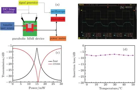
Fig.11.(a)Experimental setup for measuring DSPS MMI TO waveguide switch;(b)switch response of dual-size parabolic structural MMI TO waveguide switches;(c)actual curves of output optical power versus driving electric power for cross and bar states of the DSPS MMI TO waveguide switch at 1550 nm;(d)curve of insertion loss varying with temperature.
The comparisons of performance between fabricated switch and other reported MMI TO switches are listed in Table 1.It can be observed that our fabricated DSPS MMI TO waveguide switch can achieve larger extinction ratio and lower power consumption.
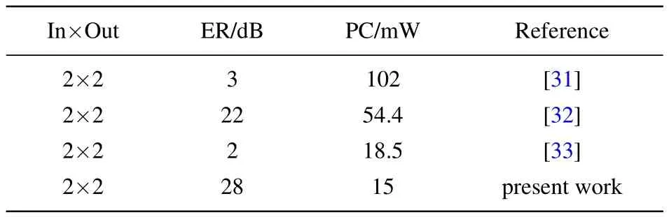
Table 1.Comparisons between our results and other published results for MMI switch.
3.Conclusions and perspectives
In this work,a DSPS MMI TO waveguide switch is designed and fabricated by using the low-loss fluorinated photopolymer materials.Comparing with the traditional DSLS MMI device,the effective length of the MMI coupling region proposed can be effectively reduced by 40%.The actual performances of the MMI switch are measured:the insertion loss is 7 dB,the switching power is 15 mW,and the extinction ratio is 28 dB.In contrast to the traditional MMI optical switches,the new type of parabolic structural MMI TO waveguide switch exhibits lower power consumption and larger extinction ratio.The compact fluorinated polymer MMI TO switches as elements are suitable well for realizing minia-turization,high-properties,and lower cost of photonic integrated circuits.
[1]Depizzol D B,Montalv˜ao J B,Lima F O,Paiva M H M and Segatto M E V 2018 Expert Syst.Appl.107 72
[2]Gou P Q,Kong M,Yang G M,Guo Z H,Zhang J,Han X F,Xiao J N and Yu J J 2018 Opt.Commun.424 159
[3]Forni F,Shi Y,Tran N C,Boom H P A,Tangdiongga E and KoonenA M J 2018 J.Lightwave Technol.36 3444
[4]Li X Y,Qin L,Li X Y,Zhang J S,Ren M Z,An J M,Yang X H and Xu X S 2017 Chin.Phys.Lett.34 034211
[5]Zhang Z J,Yang J B,He X,Han Y X,Zhang J J,Huang J,Chen D B and Xu S Y 2018 Opt.Commun.425 196
[6]Herbert D,Kumar S,Cristina L A,Mikael D,Guy L,Peter V,Jan W and Dries V T 2018 IEEE Photon.Technol.Lett.30 1258
[7]Deng Y G,Yako M,Zhang Z Y and Wada K 2018 IEEE J.Sel.Top.Quantum Electron.24 8300505
[8]Huang B J,Tsai C T,Lin Y H,Cheng C H,Wang H Y,Chi Y C,Chang P H,Wu C I and Lin G R 2018 ACS Photon.5 2251
[9]Liu Y,Sun Y,Yi Y Y,Tian L,Cao Y,Chen C M,Sun X Q and Zhang D M 2017 Chin.Phys.B 26 124215
[10]Sakamaki T,Narita Y,Tsuda H,Nakajima S and Kawanishi T 2010 IEICE Electronic.Express 7 360
[11]Shin J S,Park T H,Oh M C,Chu W S,Lee C H and Shin S Y 2015 Opt.Express 23 17223
[12]Soref R A,Francesco D L and Vittorio M N P 2018 Opt.Express 26 14879
[13]Richard A S,Francesco D L and Vittorio M N P 2018 Opt.Express 26 14959
[14]Rizal C S and Niraula B 2018 Opt.Commun.410 947
[15]Pan P,An J M and Wang H J 2015 Opt.Commun.351 63
[16]Li H Q,Dong X Y and Li E 2013 Opt.&Laser Technol.47 366
[17]Liang Y X,Zhao M S,Luo Y Q,Gu Y Y,Zhang Y,Wang L H,Han X Y and Wu Z L 2016 Opt.Eng.55 117102
[18]Guo F,Lu D,Zhang R K,Wang H T,Wang W and Chen J 2016 Chin.Phys.Lett.33 024203
[19]Ghanshyam S,Ashok S and Seema V 2013 IETE J.Res.59 479
[20]Xiao H F,Deng L,Zhao G L,Liu Z L,Meng Y H,Guo X N,Liu G P,Liu S,Ding J F and Tian Y H 2017 J.Opt.19 025802
[21]Zhang S C,Ji W,Yin R,Li X,Gong Z Y and Lv L Y 2018 IEEE Photon.Technol.Lett.30 107
[22]Le D T,Truong C D and Le T T 2017 Opt.Commun.387 148
[23]Chaudhuri R R,Amarachukwu N E,Youngsik S and Seo S W 2018 Opt.Commun.418 1
[24]Han H L,Le H,Zhang X P,Liu A,Lin T Y,Chen Z,Lv H B,Lu M H,Liu X P and Chen Y F 2018 Opt.Express 26 25602
[25]Zhang Z D,Ma L J,Gao F,Zhang Y J,Tang J,Cao H L,Zhang B Z,Wang J C,Yan S B and Xue C Y 2017 Chin.Phys.B 26 124212
[26]Zhang Z D,Zhao Y N,Lu D,Xiong Z H and Zhang Z Y 2012 Acta Phys.Sin.61 187301(in Chinese)
[27]Yu Y Y,Sun X Q,Ji L T,He G B,Wang X B,Yi Y J,Chen C M,Wang F and Zhang D M 2016 Chin.Phys.B 25 054101
[28]Kim J P,Lee W Y,Kang J W,Kwon S K,Kim J J and Lee J S 2001 Macromolecules 34 7817
[29]He G B,Ji L T and Gao Y 2017 Opt.Commun.402 422
[30]Wang J H,Chen C M,Zheng Y,Wang X B,Yi Y J,Sun X Q,Wang F and Zhang D M 2017 Chin.Phys.B 26 024212
[31]Supaat A S M,Ibrahim M H,Mohammad A B,Kassim N M and Ghazali N E 2008 Am.J.Appl.5 1552
[32]´Alvaro R,Ana G,Antoine B,Amadeu G and Pablo S2016Opt.Express 24 191
[33]Wang S P and Dai D X 2018 Opt.Lett.43 2531
猜你喜欢
杂志排行

Chinese Physics B的其它文章
- Entangled multi-knot lattice model of anyon current∗
- Miniature quad-channel spin-exchange relaxation-free magnetometer for magnetoencephalography∗
- Observing the steady-state visual evoked potentials with a compact quad-channel spin exchange relaxation-free magnetometer∗
- Quantum interferometry via a coherent state mixed with a squeezed number state∗
- Cavity enhanced measurement of trap frequency in an optical dipole trap∗
- 7.6-W diode-pumped femtosecond Yb:KGW laser∗