Development of long-wavelength infrared detector and its space-based application requirements∗
2019-02-25JunkuLiu刘军库LinXiao肖林YangLiu刘阳LongfeiCao曹龙飞andZhengkunShen申正坤
Junku Liu(刘军库),Lin Xiao(肖林),Yang Liu(刘阳),Longfei Cao(曹龙飞),and Zhengkun Shen(申正坤)
Nanophotonics and Optoelectronics Research Center,Qian Xuesen Laboratory of Space Technology,China Academy of Space Technology,Beijing 100094,China
Keywords:long-wavelength infrared detector,thermal detector,photon detector,space-based application
1.Introduction
According to Planck’s law of blackbody radiation,all objects with a temperature above absolute zero emit electromagnetic radiation.The spectral radiance,L(λ,T),can be expressed as
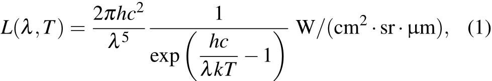
where h is the Planck’s constant,c is the speed of light,λ is the wavelength,k is the Boltzmann constant,and T is the temperature of the object.The peak wavelength λpeakof blackbody radiation is calculated with Wein’s displacement law,which is

where T is the temperature of object.Several typical temperatures are as follows:the temperature on the surface of the Sun is about 5778 K,the exhaust temperature of aero engine is about 1000 K,the temperature of human body is about 310 K,and background temperature of the universe is about 2.7 K.Table 1 lists the radiation peak wavelength of these objects.
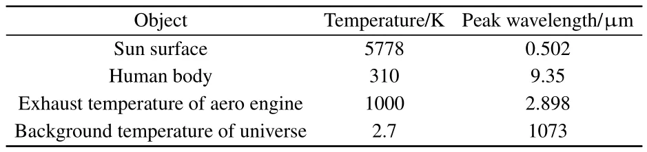
Table 1.Peak wavelength of blackbody radiation of object with different temperatures.
Blackbody radiation power from an object can be calculated by Stefan-Boltzmann equation

where A is the surface area of the object,ε is the emissivity,σ is the constant of Stefan-Boltzmann and is equal to 5.670373×10⁻⁸W·m-2·K-4,T is the temperature of the object.For human body,if A=1.2 m2,ε=1,T=310 K,and the surrounding temperature T0is 293 K,the net radiation power is Pnet=Aεσ(T4-T40)=126.6 W.
Infrared wavelength is defined as the spectral range that starts from the edge of the visible red light(∼ 0.78 µm)to 1000 µm.[1]According to Planck’s law of blackbody radiation,objects in the temperature range from about 3 K to 3800 K all show radiation peak wavelength in the infrared range,covering most of the objects in the universe.Therefore,infrared detection provides great convenience for space exploration.Whether it is on the earth or in the space,infrared detection technology has shown vast potential for a wide range of applications,including infrared communication,infrared imaging,infrared remote sensing,infrared detection,and infrared exploration.
Infrared wavelength is often subdivided into three bands:near infrared(NIR)(0.78 µm-3 µm);mid-infrared(MIR)(3µm-50µm),and far-infrared(FIR)(50µm-1000µm).According to the transmission characteristics of the atmosphere,NIR and MIR are further subdivided into short-wavelength infrared(SWIR),medium-wavelength infrared(MWIR),and long-wavelength infrared(LWIR)with the wavelength range of 1µm-2.5µm,3µm-5µm,and 8µm-14µm,respectively.The research about infrared detection technology is focused on these transmission bands.
Infrared detector is the core component of infrared detection technology.The research about infrared detector was rare before the 1940s.After World War II,increasing attention has been paid to infrared detector due to the application demands in war.Infrared detection technology has unique advantages;for example,it still works at night compared with visible detector and is a passive detection technology compared with microwave detection technology.[2]After more than 70 years of development,remarkable achievements have been made in the development of infrared detectors.Nowadays,infrared detectors made from different materials have realized detection of wavelength range from 0.75µm to 1000µm.Figure 1 shows the infrared detectors working at different wavelengths.For the detectors at NIR,SWIR,and MWIR,the detectivity has reached background limited performance[1]and the device scale extends from single element to million pixel focus plane array(FPA).[3]Table 2 summarizes the FPA status at different infrared wavelengths.The potential materials for LWIR detector are HgCdTe,[4]InAs/GaSb type-II superlattice(SL),[5,6]GaAs/AlGaAs quantum well(QW)and quantum dot(QD),[7]arsenic-doped silicon blocked impurity band(Si:As BIB),[8]VOxand a-Sibolometer,[9]and superconductor.[10]Atpresent,most of LWIR detectors work in single element or small FPA mode,still below the expectations of low noise,high detectivity,and large format LWIR detector.
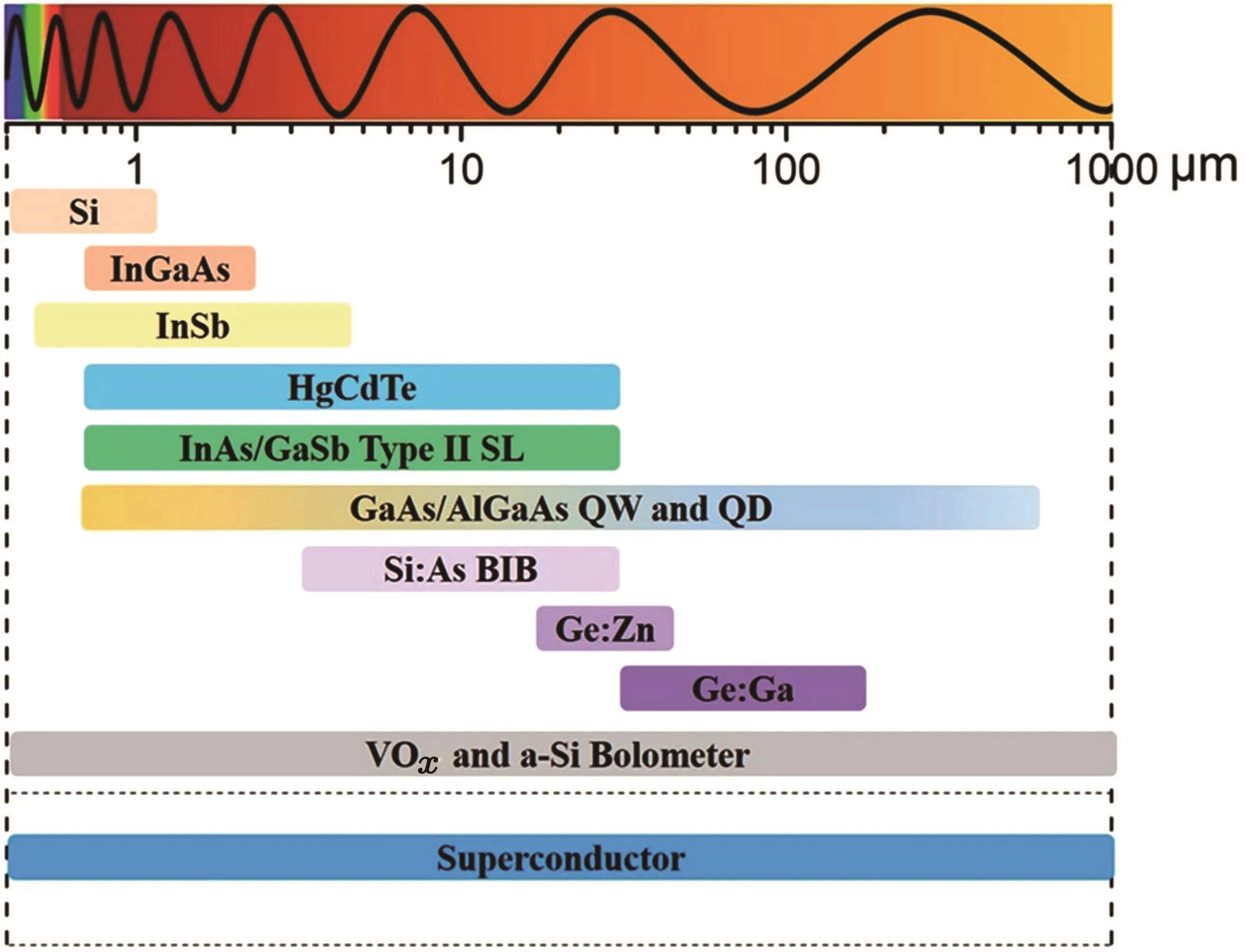
Fig.1.Potential materials working at different infrared wavelengths.
In recent years,there has been an increasing demand for long-wavelength infrared detector,which has potential application in night vision,remote sensing,astrophysics research,and space exploration.[16-19]In the field of exploring and finding earth-like planet,LWIR detectors have their unique advantages compared with detectors in other bands.In this review,we present the infrared detector technology and the developmentofLWIR detector.Afterthat,the space-based application requirements for LWIR detector and the prospects of perspective LWIR detector technology are discussed.

Table 2.The FPA status at different infrared wavelengths.
2.LWIR detector technology
2.1.LWIR detector technology
Infrared detector consists of infrared sensitive material and readout circuit.[1]Readout circuit performs the function of collection, filter,amplifying,and processing signals from the sensitive material.Almost all readout circuits are made based on the silicon material for its high performance and advanced fabrication technology,which is becoming more and more important for realizing high performance infrared detector.This is particularly true for LWIR detector,which has posed great challenges for noise,dark current,and well depth of readout circuit.[17,20]Therefore,designing and optimizing readout circuit is also an important aspect in LWIR detector research.
LWIR-sensitive material absorbs radiation and converts it into observable physical quantities.In theory,all physical phenomena related to infrared can be used as the basis of exploring infrared detectors.[21]Up to now,most of the developed LWIR detectors can be divided into two types:thermal detectorand photon detector.In recentyears,in orderto realize high detectivity and extremely low noise LWIR detector,superconductor detector and other detectors based on low-dimensional materials and novel detector architecture have been explored.
2.2.Thermal detector
When infrared radiation is absorbed by the sensitive material and induces a change in the temperature,the physical quantities depending on the temperature,such as resistance,volume,polarization,etc.,are measured.This is the mechanism of the thermal detector.Thermal detector has no wavelength selection and theoretically responds to all infrared wavelengths.Thermal detector can work at room temperature and is the most important uncooled LWIR detector.
Figure 2 shows a typical thermal detector model.[1]Cthis the heat capacity of detector and Gthis the thermal conductance between detector and supporting substrate.The supporting substrate is also the heat sink with a constant temperature T.When the infrared radiation is absorbed by the detector,its temperature rises.In a steady state,the amount of temperature rise ΔT can be calculated by solving thermal equilibrium equation
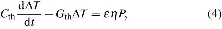
where ε is the emissivity,η is the quantum efficiency,and P is the incident radiation power.
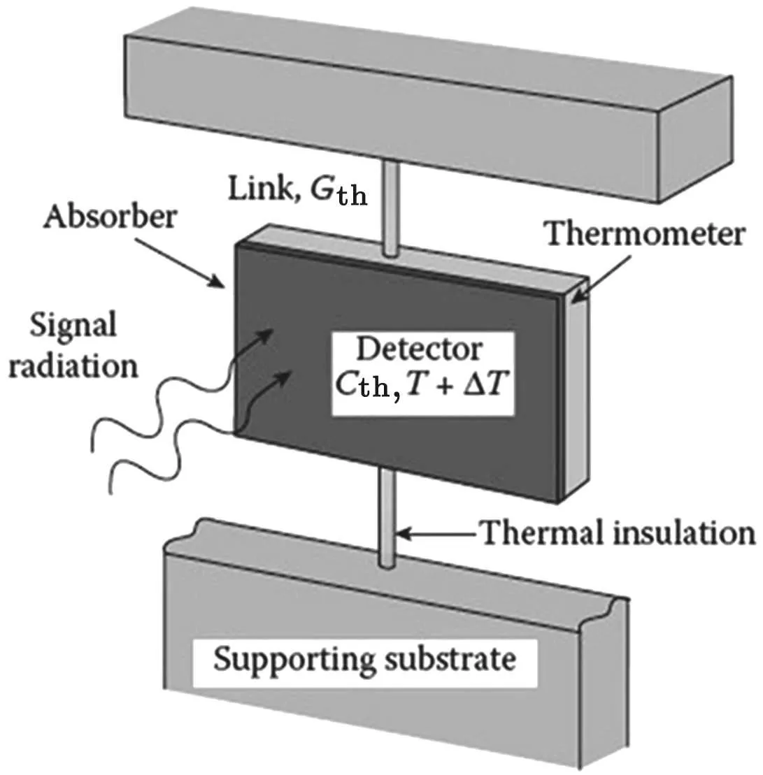
Fig.2.Illustration of a typical thermal detector model.
Assume that the incident radiation power is a periodic function,P=P0eiωt.The temperature rise ΔT is given as
The first term is the transient part and decreases to zero with time.Thus,the change of the temperature is
Since the temperature rise is inversely proportional to Cthand Gth,utilizing small Cthand Gthcan lead to large temperature rise ΔT and high sensitivity.However,considering the fact that the detector response time τ is determined by the ratio of Cth/Gth,it is necessary to make the heat capacity Cthas small as possible to avoid excessively slow response time.Therefore,a small detector mass and fine connecting wires to the heat sink are desirable.
For thermal detector,the fundamental limit on the performance comes from the thermal fluctuations in the thermal link between the heat sink and the detector.The fluctuation in the power is[1]

The value of Pfluctgives the minimum detectable power for an ideal thermal detector.Thus,the noise equivalent power(NEP)can be expresses as

where k is the Boltzmann’s constant,and T is the temperature of the heat sink.NEP will reach the smallest detectable power when Gthis at its minimum value which is equal to radiative component of the thermal conductance.For the thermal detector having a receiving area A and emissivity ε,the radiative component of the thermal conductance is
Thus the limited NEPlimitedis

For a device with pixel size of 50µm and A=250µm2,and the device is at room temperature and T=290 K,if all the incident radiation is absorbed by the detector,ε=1,η =1,and then

Other noise sources in this calculation are ignored and the NEP value in practice is larger than that of NEPlimited.
One of the most important thermal detectors is bolometer,which is a temperature-sensitive electrical resistor.[9]Its operation is based on its temperature rise caused by absorption of incident radiant energy.The change in temperature causes a change in electrical resistance,which will be measured by an external electrical circuit.When the radiation is removed,the temperature of the bolometer returns to its initial value,which is determined by the ambient surroundings in which it is immersed.If the resistance increases with the temperature,as found with metals,the bolometer is said to have a positive temperature coefficient of resistance(TCR);if it decreases as the temperature rises,as found in semiconductors under most operating conditions,it is said to have a negative TCR.
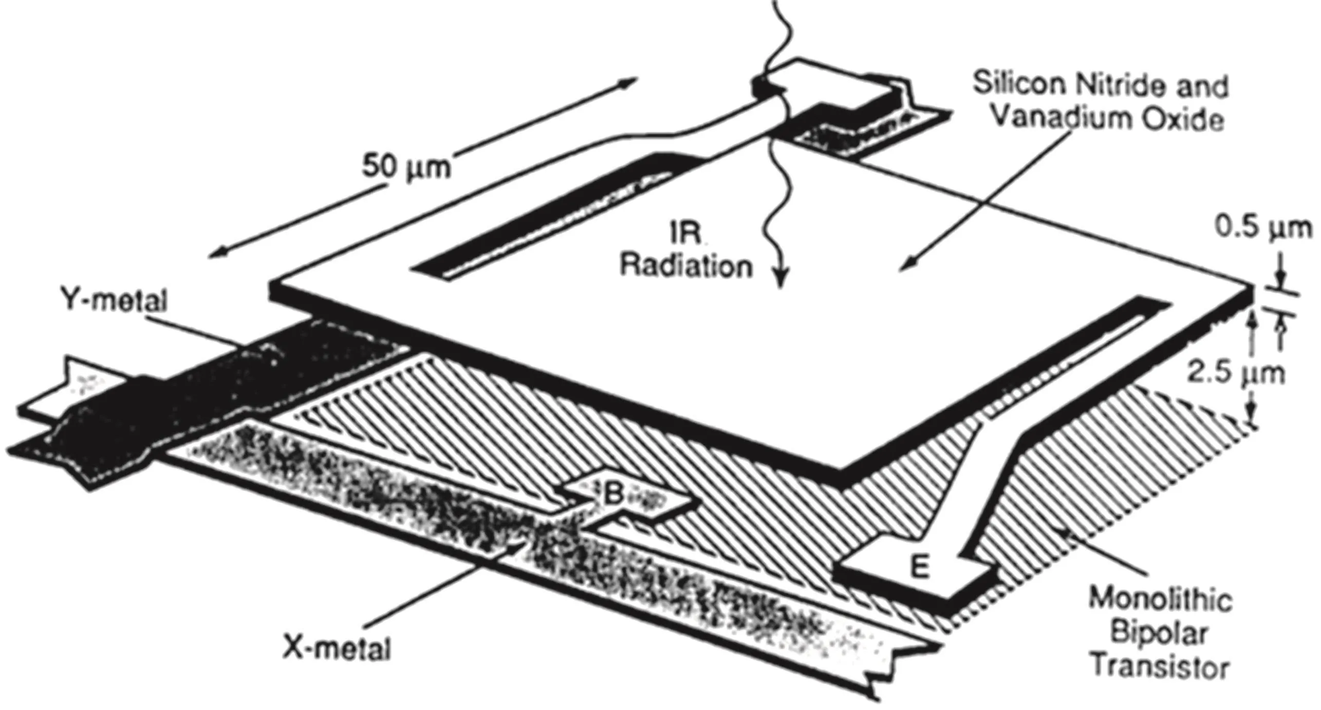
Fig.3.Microbolometer pixel structure.[9]
Modern microbolometer arrays employ a pixel structure originally developed by Honeywell,Inc.(as shown in Fig.3).[9]Itis termed a monolithic structure and is prepared by silicon micromachining.The detector part,composed of silicon nitride(Si3N4)and sensitive material,is suspended onto silicon readout circuit to decrease the thermal conductance Gthbetween detector and substrate and the thermal capacity Cthof detector area.Today,the most common bolometer temperature sensitive materials are semiconducting vanadium oxide(VOx)and amorphous silicon(a-Si),both of which have high temperature TCR and are compatible with silicon fabrication process.Microbolometers based on VOxand a-Si are the most important low-cost LWIR detectors.
Figure 4 shows a typical microbolometer FPA chip and pixel structure.The core technologies for implementing the chip include
(I)high TCR temperature-sensitive material preparation;
(II)high reliable microbridge fabrication;
(III)High performance readout integrated circuit design and fabrication;
(IV)High reliable vacuum packaging.
The first practical microbolometer device was released by Honeywell,Inc.in the 1970s,supported by the Defense Advanced Research Projects Agency(DARPA).The device is based on VOxand realizes 320×240 array size with noise equivalent differential temperature(NEDT)of 50 mK.[9]It satis fies a lot of military and civilian needs at the LWIR wavelength.Later,many countries such as France,Germany,Japan,and others started to explore bolometer-related technology.In the 1990s,there was a successive appearance of micro-bridge bolometer based on a-Si presented by France ULIS,and the p-n junction bolometer by Mitsubishi of Japan.[1]
At present,the main foreign research and production companies of microbolometer detector are:ULIS in France,FLIR,DRS,L3,BAE,and Raytheon in America,and NEC in Japan.Table 3 lists their typical FPA devices.
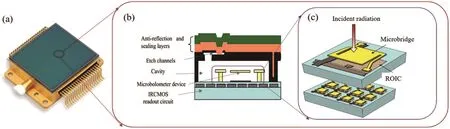
Fig.4.(a)Microbolometer FPA chip;(b)and(c)pixel structure.
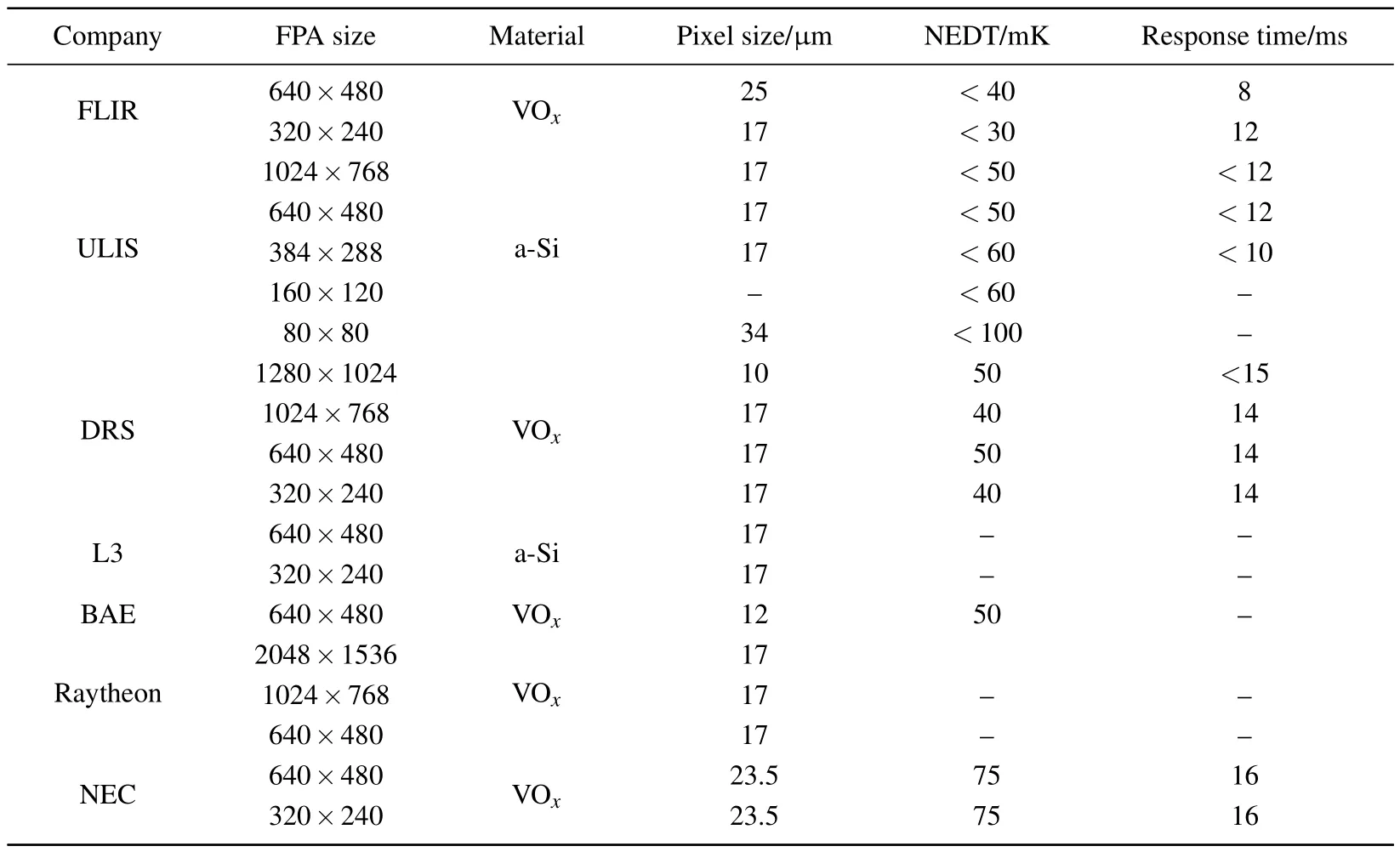
Table 3.Microbolometer FPA products from foreign companies.
From the lists of FPA in Table 3,it can be seen that the FPA size of microbolometer is mainly 640×480 or 320×240,indicating that these two specifications have been able to meet the civilian applications.Only companies with military background,such as Raytheon and DRS,continue to pursue large-scale and rapid response FPA to meet specific military needs.[15]American companies are the main research institutes in this field.This is mainly due to their advanced semiconductor technology and accumulation of technology in infrared detector research.
Before 2005,microbolometer detectors in china were mainly imported from foreign companies.However,due to the potential in military applications,the United States began to impose a strict embargo on China in such imports.In civilian applications,US manufacturers only sellthe whole thermal imager,or the core assembly with limited capabilities in the resolution and frame frequency.In recent years,with the development of micro-electromechanical systems(MEMS)and application specific integrated circuit(ASIC)technology in China universities,including Tsinghua University,Huazhong University of Science and Technology,University of Electronic Science and Technology,and Tianjin University,have gradually begun to study microbolometer infrared detector.Starting from 2006,commercial companies,including Dali Technology,North Guangwei Technology,IRay technology,Guide infrared technology,and other large-scale thermal imager manufacturers,have also begun to develop microbolometer infrared detectors.Table 4 lists their released FPA devices.The released product data show that their performance has reached the same level of their overseas counterparts.
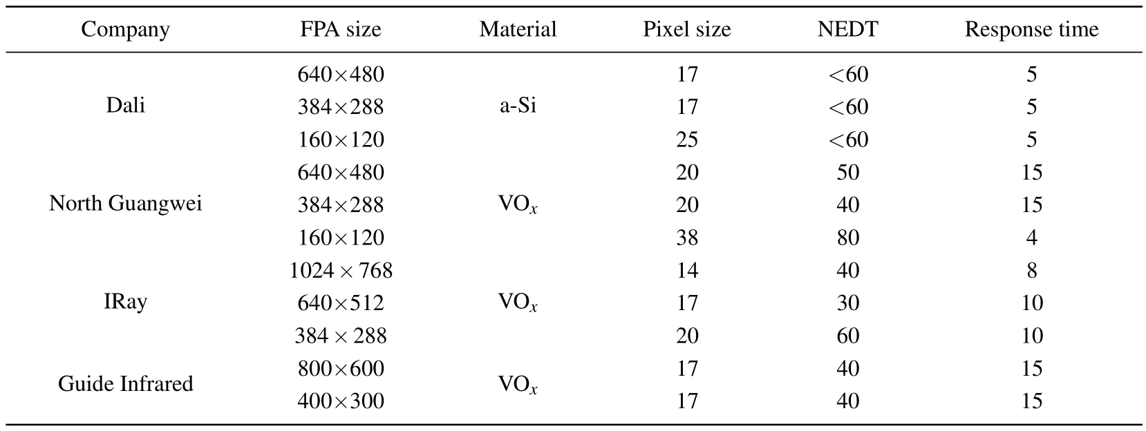
Table 4.Microbolometer FPA products from Chinese companies.
Thermal detectors have the advantages of being costeffective,with no need to be cooled,and highly compatible with silicon fabrication process;however,its detectivity is lower than 109cm·Hz1/2/W and the response time is longer than a millisecond.It is mainly suitable for detection of low speed objects at short range,and one possible application for thermal detector is being used as a payload on the lander to explore asteroids in space exploration.
2.3.Photon detector
In photon detector,the infrared radiation is absorbed within the material by interaction with electrons either bound to lattice atoms or to impurity atoms,or with free electrons,which produces excited electrons of high energy.The observed electrical output signal results from the changed electronic energy distribution.The fundamental optical excitation processes in semiconductors are illustrated in Fig.5.[1]
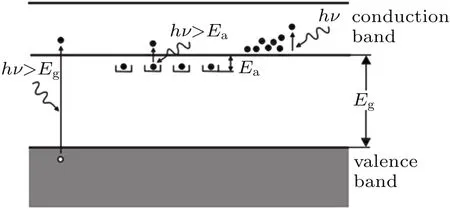
Fig.5.Fundamental optical excitation processes in semiconductors.
For a photon detector,the spectral current responsivity Riis defined as[1]
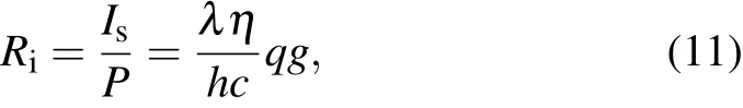
where λ is the incident wavelength,η is the quantum efficiency,h is the Planck’s constant,c is the speed of light,q is the electron charge,g the device gain,and P is the incident infrared power.Isis the photoinduced current and can be expressed as Is=qηΦg,in which Φ is the photon number and can be expressed as P=Φhλ/c.
The responsivity depends on the device area and the integral time.Specific detectivity D∗,normalized per square root of the device’s area and frequency bandwidth,is introduced as a figure of merit and is defined as[1]
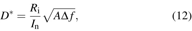
where A is the area of the photosensitive region of the detector,Δf is the frequency bandwidth,and Inis noise current.The noise sources include thermal noise,shot noise,generationrecombination noise,background noise,etc.[22]For photon detectors working in different modes,such as photoconductor and photovoltaic mode,and for different conditions,there are different noise levels.Therefore,the specific detectivity D∗depends on the nature of the device and its working condition.
Compared with thermal detector,the photon detector exhibits a selective wavelength dependence of response.Its cut-off wavelength at infrared end is determined by λ=1.24/Eg(eV)µm,where Egis the bandgap or sub-bandgap in semiconductor.Photon detector exhibits good signal-tonoise performance and fast response.However,in order to achieve this,the photon detector requires cryogenic cooling,a necessary process to prevent the thermal generation of charge carriers,which may compete with the optical ones,increasing the noise level of the devices.Depending on the nature of the interaction,the class of photon detectors is further sub-divided into different types,of which intrinsic detector,extrinsic detector,photo-emissive(Schottky barriers),quantum well,and quantum dot are the most important ones.[1]
2.3.1.Intrinsic detector
When infrared radiation is absorbed by semiconductor,it excites electrons from the valance band to the conduction band,and the material that demonstrates this property is called intrinsic detector.At present,intrinsic infrared detector working at LWIR band includes Hg1-xCdxTe,[4,23]PbSnTe,InAsSb,and InAs/GaSb SL.PbSnTe has little application due to its high dielectric constant and high thermal coefficient of expansion,which results in the long response time and mismatch with silicon technology.The other three materials are introduced in the following part.
(i)Hg1-xCdxTe infrared detector
Hg1-xCdxTe alloy is a variable direct band gap semiconductor,which is developed by Lawson et al.in 1959.[23]Its energy gap extends from zero to 1.5 eV by varying the component of Hg and Cd(see Fig.6).This provides an unprecedented degree of freedom in infrared detector design.At present,Hg1-xCdxTe is the most widely used LWIR photodetector.
In order to realize high performance photon detector based on Hg1-xCdxTe alloys,high quality single crystal Hg1-xCdxTe alloys are needed.It is difficult to prepare high quality single crystal Hg1-xCdxTe because a relatively high Hg pressure is present during growth,which makes it difficult to control the stoichiometry and composition of the material grown.Early experiments and a significant fraction of early production were done using a quench-anneal or solid-state recrystallization process.[4]In the 1980s,liquid phase epitaxy(LPE)Hg1-xCdxTe on CdTe substrate was realized,[24]which opened the door to fabricate Hg1-xCdxTe FPA device.The growth of Hg1-xCdxTe on CdZnTe substrate by LPE has become the most mature method to prepare single crystal Hg1-xCdx.But its size is still limited by the existing CdZnTe substrate.
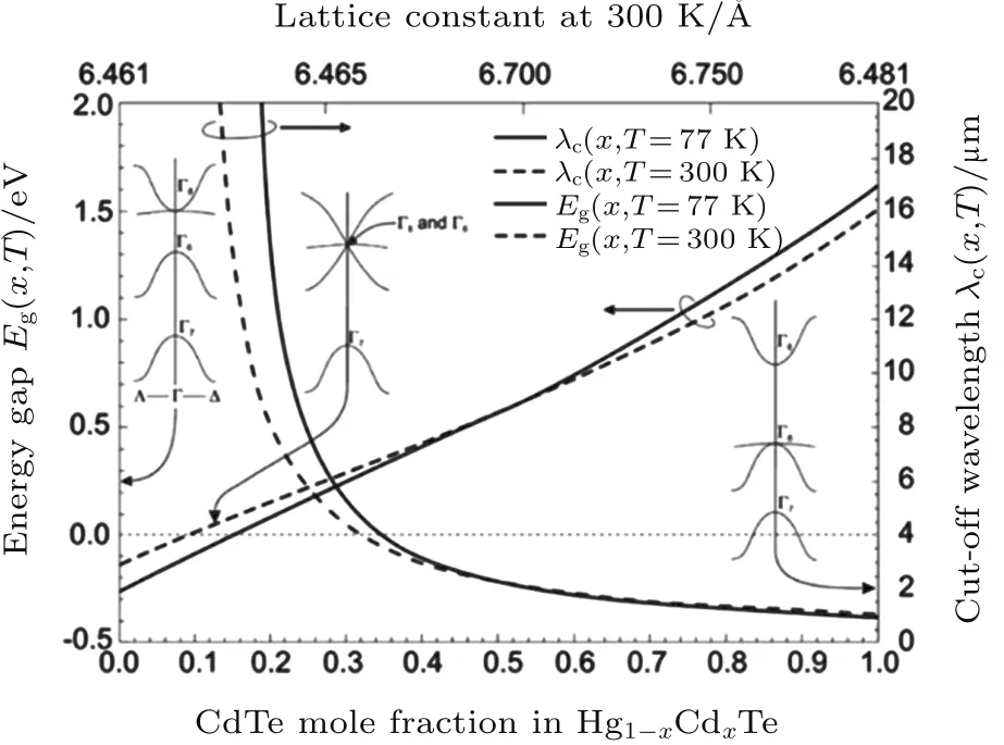
Fig.6. The band gap and the corresponding cut-off wavelength of
Since then,various vapor phase epitaxy(VPE)growth methods,including metal-organic chemical vapor deposition(MOCVD),molecular beam epitaxy(MBE),and their derivatives,have been used to prepare single crystal Hg1-xCdxTe.The VPE growth of Hg1-xCdxTe is typically conducted by nonequilibrium methods,which can dynamically modify the growth conditions during the growth to tailor band gaps,add or remove dopants,prepare surfaces and interfaces,add passivation,perform anneals,and even allow the growth on selected areas of a substrate.The growth control is exercised with great precision to obtain basic material properties comparable to those routinely obtained from equilibrium growth.At present,it has been realized to grow epitaxy Hg1-xCdxTe on Si,[25]Ge,[26]and GaAs[27]substrate,which makes it possible to realize large formant FPA.
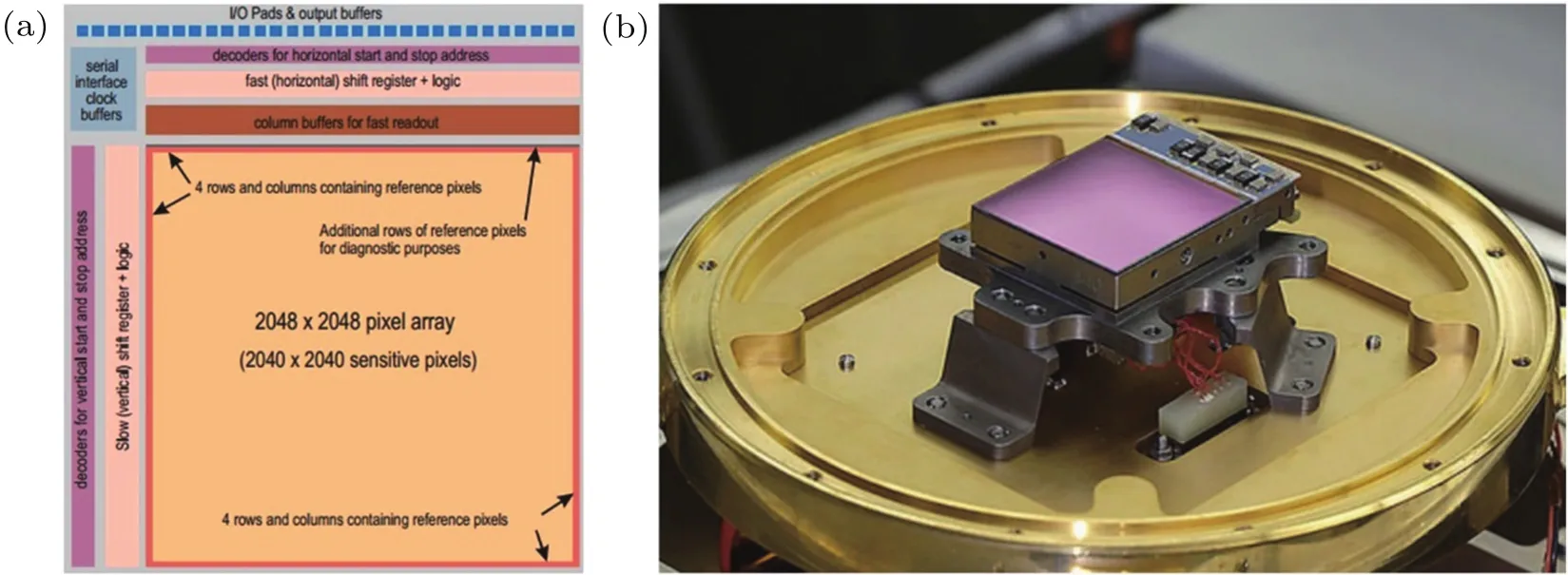
Fig.7.(a)Block diagram and(b)photograph of 2048×2048 pixel Hg1-x Cd x Te FPA.[12]
Now,the array size as large as 2048×2048 has been realized by Teledyne technology and Raytheon company in MIR(< 5 µm).[17]Figure 7 shows the block diagram and photograph of Hg1-xCdxTe FPA made by Teledyne.[12]Considering that it is difficult for the detector to work at long-wavelength,most released LWIR detectors are single element.This is because of the non-uniformity of Hg1-xCdxTe,which causes severe changes in the cutoff wavelength.Thus,it is desirable to explore new photodetector material to replace Hg1-xCdxTe in the long-wavelength range.
(ii)InAs1-xSbxinfrared detector
InAs1-xSbxis also a variable direct band gap semiconductor by means of varying the component of As and Sb(see Fig.8).[28]Its minimum bandgap can be as low as 0.1 eV when x=0.65.Compared with Hg1-xCdxTe,InAs1-xSbxhas strong covalentbond and exhibitsimportantadvantages:betterstability,higher electron and hole mobilities,and high-quality and low-cost substrates,making it possible to realize room temperature LWIR detector.
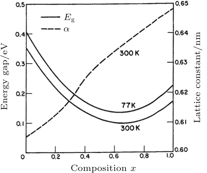
Fig.8.The band gap and lattice constant of InAs1-x Sb x alloy.[28]
In theory,InAs1-xSbxhas comparable performance to Hg1-xCdxTe.[29]But InAs1-xSbxfilm prepared by MBE[30]and melt epitaxy[31]shows short minority lifetime for the Shockley-Read-Hall recombination under the present conditions.The device performance is worse than Hg1-xCdxTe at low temperature and comparable to the thermal detector at room temperature,[32,33]whereas its response time is better than the thermal detector.In this regard,more work is needed to improve the material quality in the future.
(iii)InAs/GaSb-type-II superlattice
Figure 9 shows the band-structure of InAs/GaSb type-II superlattice.[34]In this material,the electrons in valence miniband of GaSb can be excited to conduction miniband of InAs.Furthermore,the position of valence miniband in GaSb and conduction miniband in InAs can be modified by varying the thickness of GaSb and InAs according to the quantum confinement effect.Theoretically,the band gap can vary continuously in the range from 0 meV to about 400 meV.[5]It is suitable to realize the photodetector at MWIR and LWIR.

Fig.9.Band-structure of InAs/GaSb type-II superlattice.
InAs/GaSb type-II superlattice was proposed by Sai-Halasz et al.in 1977,[34]and it was explored as infrared detector by Smith et al.in 1987.[35]Compared with Hg1-xCdxTe and InAs1-xSbxbulk infrared detector,InAs/GaSb type-II superlattice has comparable absorption coefficient,reduced Auger recombination,and mature material growth technique,which makes it promising to realize high performance LWIR detector.[5]Experimental data have shown that the detectors have response from NIR to 32µm.[36]In 2010,both Jet Propulsion Laboratory(JPL)and Northwestern University realized 1024×1024 large-format LWIR FPAs using this material.[12,37]InAs/GaSb type-II superlattice demonstrates clear advantage compared with other materials in LWIR and VLWIRband.The LWIRdetectorbased on InAs/GaSb type-II superlattice has been transferred to application in America.[38]Figure 10 shows a 4-inch(1 inch=2.54 cm)InAs/GaSb type-II superlattice wafer with GaSb as substrate fabricated by Hughes Research Laboratories(HRL)supported by U.S.Army ManTech funding.
InAs/GaSb type-II superlattice is promising for large format LWIR and VLWIR detector. Therefore,Jianxin Chen’group from Shanghai Institute of Technical Physics and Zhichuan Niu’s group from Institute of Semiconductors in China have started to focus on exploring infrared device based on InAs/GaSb type-II superlattice since 2005,[39-42]whose work shows promising application prospects in the future.In order to realize high performance InAs/GaSb type-II superlattice detector,fabrication of clear superlattice interface,reducing dark current,increasing carrier lifetime,and realizing surface passivation are needed.
2.3.2.Extrinsic detector
In addition to utilizing the intrinsic band gap of semiconductor materials,detectors have employed the energy levels associated with dopants in semiconductors,in which electrons are excited to conduction band or holes are excited to valance band.These extrinsic infrared detectors are mostly based on Si and Ge with benefits from the advanced materials and devices fabrication technology.Extrinsic photon detectors are used in a wide range of the IR spectrum extending from a fewµm to approximately 500 µm as shown in Fig.11.[43]Si:As BIB is one of the most important extrinsic LWIR detector,and it has response from MWIR to 30µm.[8,20]Compared with intrinsic LWIR detector,Si-based extrinsic LWIR detector is compatible with complementary metal-oxide-semiconductor(CMOS)process and is convenient to realize large format LWIR FPA.The extrinsic IR detectors based on Si and Ge have been successfully applied to space telescope.[16,20]
2.3.3.Schottky barriers detector
Schottky barriers based on silicon can also realize LWIR detector.Its photon response can extend to red end wavelength of 15µm.[1]It has the advantages in uniformity and compatibility with CMOS process.Japanese researchers have done a lot of work in this field and applied the LWIR detector in space,[44]Due to its low quantum efficiency and extremely low working temperature,Schottky barriers LWIR detector has little application at present.
2.3.4.Quantum well and quantum dot detector
When an electron or a hole is confined in a potential well,its energy distribution becomes discrete energy level and the energy level depends on the potential well width.According to this theory,energy gap in LWIR can be designed and fabricated.This is the mechanism of quantum well and quantum dot detector.
GaAs/AlGaAs is one of the most important quantum well materials.[7]Its band-structure is shown in Fig.12.GaAs/AlGaAs has been explored to realize LWIR detector for its controllable fabrication and material uniform.In the quantum well detector,electron is excited from low level to high level in conduction band or hole is excited from low level to high levelin valence band.Itisan intraband transition process.In order to satisfy the conservation of energy and momentum during theintraband transition process,the incident light at normal incidence for quantum well cannot be absorbed.For this reason,random grating is used to create a nonzero polarization component in the quantum well direction and enhance infrared absorption in quantum well detector.[7]
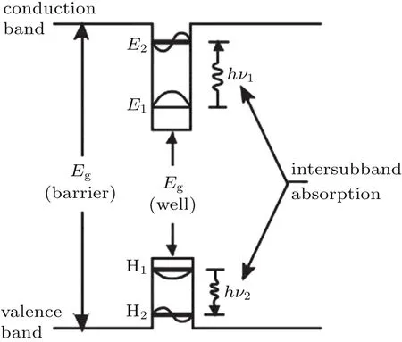
Fig.12.Band-structure of GaAs/AlGaAs quantum well.
Although the quantum efficiency of GaAs/AlGaAs quantum well detector is lower than that of Hg1-xCdxTe,its high uniformity and stability make it more desirable in LWIR FPA.A 1024×1024 large-format LWIR FPAs have been applied in Landsat satellite.[13]
Quantum dot is artificial atom that has discrete energy level depending on the QD size.QD has the potential to realize LWIR detector,but it is difficult to realize uniform QD fabrication,which limits its application.
2.4.New concept IR detector
Remarkable achievements have been made in thermal and photon detectors at LWIR,which can satisfy most application requirements.Because detectors with present noise level and detectivity are still unable to sense remote dim objects in space,new concept infrared detectors with low noise and high detectivity have always been the research focus in LWIR.Superconductor detector and plasmonic-assistant semiconductor photodetector are current research hotspots in this field.
2.4.1.Superconductor detector
Superconductivity is discovered by Kamerlingh Onnes in 1911.[45]Its resistance goes essentially to zero when it is cooled to below a certain “critical”transition temperature Tc.Figure 13 shows the superconductivity properties of Hg.[45]Based on this steep temperature sensitivity,researchers have explored a variety of superconductivity-based detectors,including superconducting nanowire single-photon detectors(SNSPD),[46]transition-edge sensors(TES),[47]superconducting tunnel junctions(STJs),[48]and microwave kineticinductance detectors(MKID).[49,50]Superconducting detectors need to operate significantly below room temperature.And various noise sources are strongly suppressed at such low temperature.Therefore,superconducting detector can realize extremely high detectivity compared with semiconductor photodetector.
i)SNSPD
A typical SNSPD consists of a∼5-nm thick and∼100-nm wide superconducting wire(Fig.14(a)).It locally switches from the superconducting to normal resistive state in response to the absorption of single photons(Figs.14(b)-14(e)).[46,51]The wire is cryogenically cooled below Tc,and shows superconducting properties.When a photon is absorbed by the superconducting film,a small and localized region known as a hot spot is created.Within such a hot spot,the temperature of the electrons is sufficiently elevated to disrupt the superconductivity and return the material to its normal resistive state.
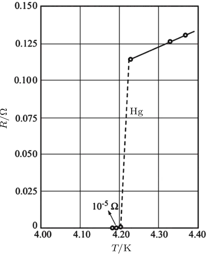
Fig.13.Resistance vs.temperature of Hg.[45]
At present,SNSPDs have demonstrated detection efficiencies above 90%in communication band.[52,53]SNSPD working at LWIR has not been reported.According to its photo-response mechanism,LWIR detector based on superconducting nanowire is potentially available in the future and its noise level can be reduced greatly and its efficiency can be further enhanced.The main difficulties are from the cooling and signal readout for array size device.
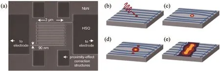
Fig.14.(a)The scanning electron microscope(SEM)image ofa typicalSNSPDmade from NbNand(b)-(e)the photo-response mechanism of SNSPD.[46,51]
ii)TES
TES was first demonstrated by Andrews in 1942,[47]which consists of a thin superconducting film working exactly at the temperature of its superconducting-to-normal resistive transition.It operates as a bolometer detecting the change in temperature after it absorbs electromagnetic radiation.This process can detect radiation from sub-mm wavelengths to gamma-rays.A very sharp transition is required in order to obtain a large electrical response to a small temperature change,making it possible to achieve extreme high sensitivity.At present,the most successful optical TES sensors can operate below 1 K,and most of the devices work at sub-kelvin.[54]For TES application,high quality material is needed to realize a very sharp transition edge.Signal readout and stable cooling also pose challenges in TES application.
iii)STJs
STJ is a sandwiched structure consisting of two superconducting films and a thin insulator barrier,[48]as shown in Fig.15(a).The top film is an absorbing layer and the bottom film is a base layer for signal collection.The incident photon excites quasiparticle in the top film,and these quasiparticles tunnel from the top absorbing layer to the bottom base layer and create net current(as shown in Fig.15(b)).STJ is the pioneering technology in superconductor-based single-photon detection and exhibits superior detection performance for photons.Breakthroughs in materials science and junction fabrication technology are needed to realize high performance STJs.
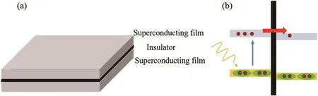
Fig.15.A schematic diagram of(a)STJs structure and(b)operation principle.
iv)MKID
MKID also detects the absorption of a photon by sensing the quasiparticles generated in a superconductor.[49]However,in this kind of detector,the number of quasiparticles is measured by the small change in the superconductor’s kinetic inductance.This is accomplished by integrating every strip of superconductor into a microwave resonant circuit(see Fig.16(b)),and monitoring the phase of a signal transmitted through the resonator(Fig.16(a)).Its advantage is that its built-in frequency domain multiplexes at GHz frequencies,allowing thousands of detectors to be read out through a single transmission line(Fig.16(b)).[50]Figure 16(c)shows a photograph of MKID array device.
Many studies have been conducted in exploring the MKID in high energy particle detector,[55]visible to NIR detector,[56]and far-infrared to millimeter-wave detector.[57]The device noise equivalent powers can reach 4.4×10⁻²⁰W/Hz1/2,[58]and this NEP value is far below what can be realized in semiconductor detector.MKID is a promising high detectivity detector,and a number of cameras for ground based telescopes have been developed including the Caltech submillimeter telescope(CSO),the Atacama path finder experiment(APEX),and the Institute for Radio Astronomy in the Millimeter Range(IRAM).[59]MKID can naturally be used to detect LWIR radiation with high detectivity.However,it suffers from a large pixel size compared with infrared wavelengths,a severe handicap in imaging technology.
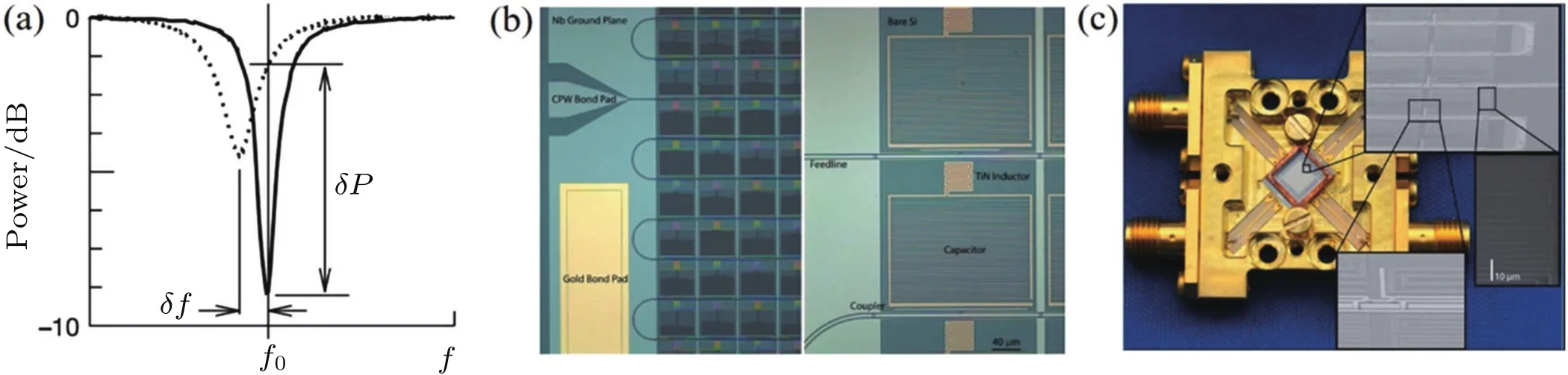
Fig.16.MKID array device and it operating principle.[49,50]
2.4.2.Plasmonic-assistant semiconductor photodetector
Plasmonic structure has the ability to concentrate light into deep-subwavelength volumes and enhance the lightmatter interactions.[60]One of its advantages is its ability to shrink the size of conventional photodetectors using plasmonic structure.Reducing detector size would lead to increased speed,decreased noise level,and enhanced detectivity.Therefore,plasmonic-assistant semiconductor photodetectors are particularly promising.
The ability of plasmonic structures to efficiently concentrate light into a deep subwavelength detector region has been demonstrated in Si[61]and Ge[62]detector as shown in Fig.17.The detector photo-response is enhanced more than a factor of 20 and the device active volume is shrunk to a volume of 10-4λ3.

Fig.17.Plasmonic-assistant(a)Si and(b)Ge photodetector.
Plasmonic based on metal has resonant peaks in the ultraviolet or visible band.It is necessary to develop suitable materials and methods to apply plasmonics to infrared detector.Two approaches have been developed to enhance the performance of infrared detector.The first approach is based on the use of transparent conductive oxide(TCO),such as indium tin oxide,or zinc oxide doped with aluminum or gallium.[63]An ab initio simulation of mercury cadmium telluride infrared detector with TCO plasmonic particles shows that the specific detectivity of the device is simultaneously enhanced by optical field localization and noise suppression.[64]The second approach is based on the use of metallic extraordinary optical transmission(EOT)arrays deposited on photodetector surface.[65]
More work needs to be done to realize high performance infrared detector assisted with plasmonic.Exploring materials with low lossand compatible with infrared devicesare desired.Plasmonic also offers the possibility to controllight field,making itpossible to realize pixelfunctionality,including polarization,wavelength selectivity,and phase adjustment.It will be a research hotspot in infrared detector field in the future.
3.Space-based application of LWIR detector
As mentioned above,a lot of objects in universe have emission peaks in long-wavelength.Therefore,long wavelength infrared detection is essential to understand many key topics and processes on the earth and in the universe.
3.1.Remote sensing
LWIR remote sensing for the earth surface can provide essential data contribution for weather,climate,and environmental monitoring. They support public and private decision-making and generate important socio-economic benefits. Therefore,meteorological satellites,such as FENGYUN-4 from China and Landsat-8[13]from America,have LWIR payload to monitor atmospheric environment,including cloud,water vapor,and temperature.The LWIR payload on FENGYUN-4 covers the wavelength range from 8µm to 13.8µm with spatial resolution of 4 km.Advanced land observation satellite-2(ALOS-2)from Japan has developed uncooled LWIR payload to monitor forest fires and volcanoes.[66]
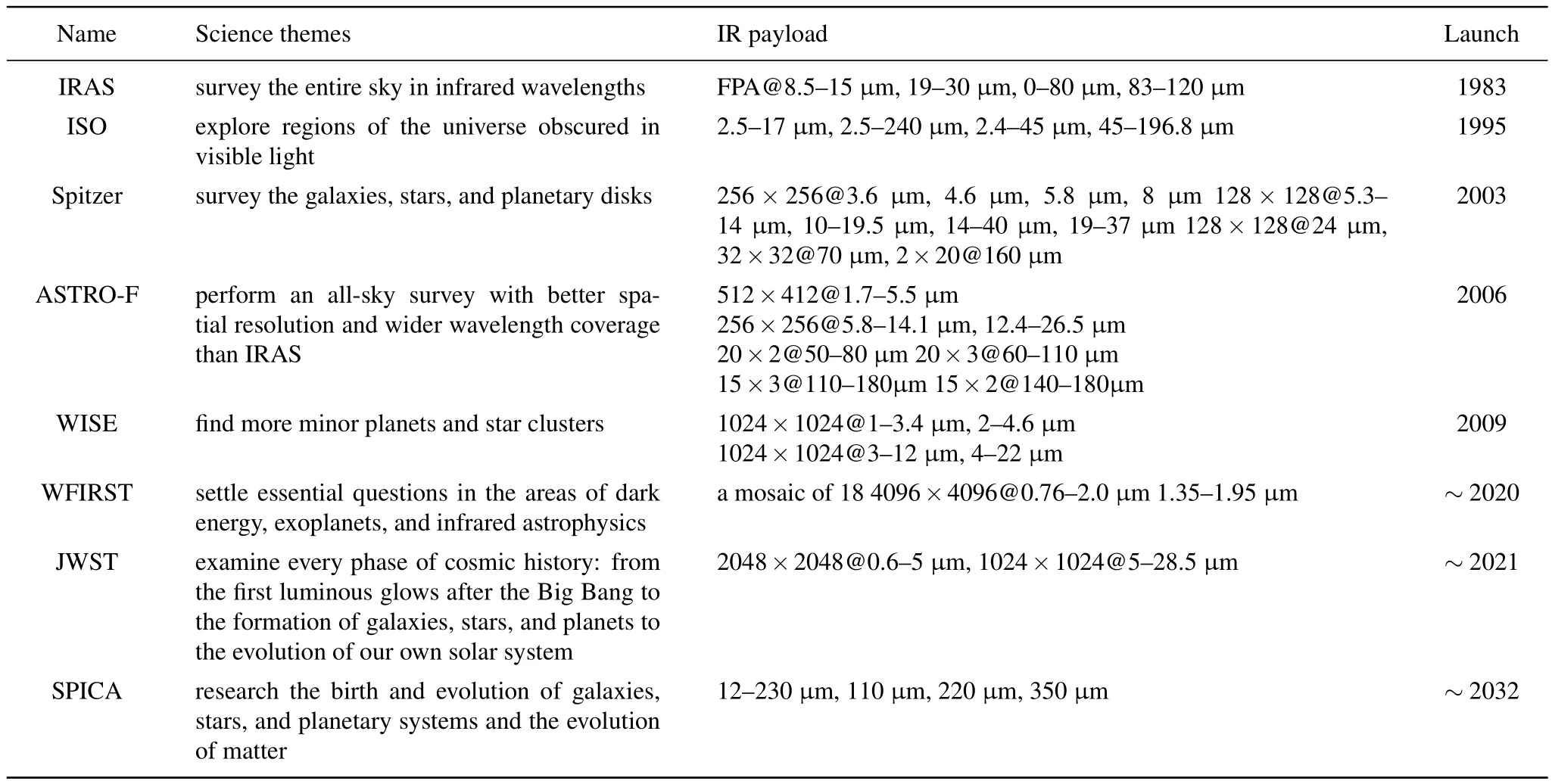
Table 5.Space telescopes with LWIR infrared payload and their science themes.
LWIR remote sensing can also be used to explore nature resource,butitneeds more sensitive and higherresolution payload for the long-distance and weak radiation intensity.Besides,it requires low noise level,high detectivity,and large format LWIR FPA detector.Locating and identifying dim and distant objects by LWIR remote sensing is necessary for space situational awareness in order to realize security earlywarning.It also requires low noise level,high detectivity,and large format LWIR FPA.
3.2.Space science research and space exploration
LWIR region of the electromagnetic spectrum contains a wealth of astronomical information.That range covers the radiation from planetary atmospheres,the interstellar medium,star formation,stellar evolution,galaxies,and the distant universe.The development of LWIR technology has greatly expanded the study of fundamental astrophysical problems.[16]Table 5 lists the major space telescopes with LWIR infrared payload and their science themes so far.
The James Webb space telescope(JWST)is one of the most famous space telescopes with LWIR detector as a core payload.Its science themes is to examine every phase of cosmic history:from the first luminous glows after the Big Bang to the formation of galaxies,stars,and planets then to the evolution of our own solar system.[67]The LWIR detectors in JWST are 1024×1024 Si:As extrinsic photodetectors(Fig.18).Table 6 shows its parameter requirement.[20]
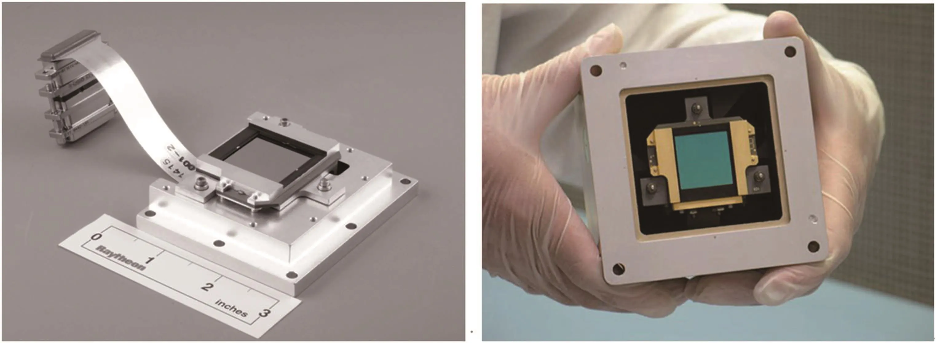
Fig.18.1024×1024 Si:As extrinsic photodetector FPA.[20]
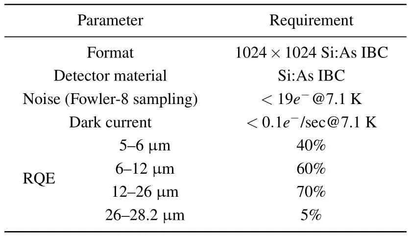
Table 6.The parameter requirement for JWST.[20]
4.Summary
After more than 70 years of development,infrared detector technology has made great progress.Remarkable achievements have been made in infrared material,device fabrication,readout circuit,and device package.LWIR detectors have been made based on the thermal resistive effect,photoelectric effect,etc.The available high performance LWIR detectors are limited,especially for large format LWIR FPA detectors.Low level noise,high detectivity,and large format LWIR detectors are prerequisites for space-based applications.InAs/GaSb type-II superlattice and silicon-based extrinsic detector are most promising materials to realize high performance LWIR detector.Digital readout circuits have the advantage ofenhancing the performance of LWIRdetectorand are becoming more and more important.At the same time,exploring system-on-a-chip for LWIR infrared FPA offers great benefits in lowering the noise level of LWIR detector.Therefore,more work needs to be done to realize high performance LWIR detectors and explore new concept of LWIR detectors in order to improve the development of space-based LWIR detection technology.
猜你喜欢
杂志排行

Chinese Physics B的其它文章
- Physics of quantum coherence in spin systems∗
- Recent progress of infrared photodetectors based on lead chalcogenide colloidal quantum dots∗
- Progress in quantum well and quantum cascade infrared photodetectors in SITP∗
- Recent advances in Ga-based solar-blind photodetectors∗
- Transition of photoconductive and photovoltaic operation modes in amorphous Ga2O3-based solar-blind detectors tuned by oxygen vacancies∗
- Ultrasonic backscatter characterization of cancellous bone using a general Nakagami statistical model∗