Electron Transport Properties of Graphene-Based Quantum Wires∗
2018-12-13HuaZhao赵华XiaoWeiZhang张小伟XiaoChunLiu刘晓春YongZheng郑勇andWanGuoLiu刘晚果
Hua Zhao(赵华), Xiao-Wei Zhang(张小伟),Xiao-Chun Liu(刘晓春),Yong Zheng(郑勇),and Wan-Guo Liu(刘晚果)
School of Physics and Electronics,Qiannan Normal University for Nationalities,Duyun 558000,China
AbstractWe study the electronic transport in quantum wire structures made of graphene.By using the nonequilibrium Green function method,the transmission is studied for varies sizes samples.Our results show that the transmission sensitive depends on the size of the system and exhibits fluctuations due to the mismating of propagating modes between the central region and the leads.The number of resonant transmission peaks increases with the increase of length of the wire,while the width of the leads mainly affect the transmission in the region of low energy.A central energy gap in the transmission spectrum is more likely to appear in the quantum wire system than in the uniform armchair graphene nanoribbons.Moreover,the energy gap can be widened for a certain size of the quantum wire system by changing the width of the leads.These results may have potential applications in designing graphene-based devices.
Key words:graphene,quantum wire,transmission
1 Introduction
Graphene,a single layer of carbon atoms arranged in a honeycomb lattice,has attracted a lot of scientific attention these years.[1−2]It is a promising candidate of nano-electronic materials due to its electronic,thermal and transport properties.[3]For example,a graphene p−n junction has been realized experimentally and can be superior to their Si-based counterparts.[4]The spindependent electron transport properties in single and doublenormal/ferromagnetic/normalzigzaggraphene nanoribbon junctionshavealso been investigated.[5]Graphene is expected to have extensive applications in the future nanoelectronic devices.Graphene sheets are zero gap materials and usually need to cut into graphene nanoribbons(GNRs)by using a variety of technologies such as lithography[6]to build the nanoelectronic devices.The presence of edges makes the electronic structure of GNRs different from that of graphene sheet due to the lateral confinement,such as the opening of band-gaps.Two types of edges are usually considered,say,armchair and zigzag.[7]The properties of GNRs can range from metallic to semiconducting according to their widths and edges.It is predicted that all zigzag GNRs(ZGNRs)are metallic,while armchair GNRs(AGNRs)are either metallic or semiconducting depending on their exact widths.[7−8]AGNRs,when semiconducting,have an energy gap scaling with the inverse of the AGNRs width,[9]which is supported by experiments.[10]
With the development of fabricating technology of GNRs,the electronic and transport properties of various GNR structures have been studied and many interesting results have been obtained recent years.Coherent transport of narrow ZGNRs with several kinds of structural constrictions has been studied,[11]and an electrostatic method of valley polarization has also been proposed based on graphene nanoconstrictions.[12]GNR junctions with L-shaped,T-shaped,and Z-shaped were proposed a few years ago.[13−14]Chen et al. studied the transport properties of a Z-shaped GNR and found that the conductance and the bound states of the system were very sensitive to the geometric structure.[15]Huang et al.studied the transmission of graphene rectangular quantum dots and demonstrated the transmission fluctuations,which depended on the size of the dot.[16]The effect of lead position on conductance fluctuations in the system was also investigated.[17]A recent study suggested that a step-like ZGNR devices showed better conductive capability than the perfect ZGNR without step.[18]In a word,the electrical properties of GNR structures strongly rely on their sizes,geometries,and edge structures.
In order to open a band gap in graphene,it has been suggested to cut the graphene into narrow AGNRs.However,wider electrodes for the system may better meet the requirements of experiments and applications.In this work we study the transport properties of graphene-based quantum-wire like structures,formed by a narrow AGNR connected two semi-in finite wider AGNR leads.To be concrete,we focus on the structure with a rectangular geometry and has a top-bottom symmetry,as shown in Fig.1.Due to the mismatch of transmitting modes between the leads and the central region,the size of each segment of the system has significant in fluence on the transport properties,especially on the energy gap.Using the non-equilibrium Green function(NEGF)method,the electron transmission probabilities are numerical calculated.We find that the transmission of the quantum wire typically exhibits fluctuations as the electron energy changes.The system is more likely to show semiconducting phase and the energy gap width is completely determined by the widths of the wire and leads.This may have potential applications in the designing of graphene nanodevices.
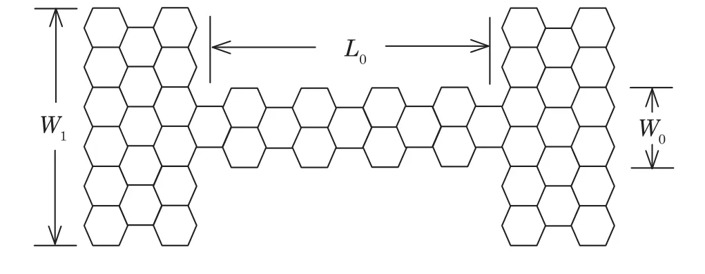
Fig.1 Schematic view of a graphene quantum wire with armchair boundaries.
2 Model and Method
In general,the system as shown in Fig.1 can be divided into three parts:left lead,device,and right lead.The two leads are assumed to be semi-in finite and are not directly contacted.The conductance G of the device can be obtained by the Landauer formula,at low temperature it can be expressed in the form
where T is the transmission probability of an electron in the graphene quantum wire.In the following of the paper,we use transmission T to discuss the transport properties of the system,because it is simply proportional to the conductance G.Here we use the tight-binding model and employ the NEGF formalism to calculate the transmission T.[16]
In the tight-binding representation,the Hamiltonian of the device can be written as
where ϵiis the on-site energy,and ciare the creation and annihilation operators at site i,t is the nearest hopping integral,and 〈i,j〉stands for the nearest hopping pair.It should be noted that the device is chosen to include all the irregular parts so that the left and right leads are uniform in the width.[16]The Green function of the device is defined as

where ΣL,Ris the self-energy of the left or right lead,iη is a small imaginary term added to make the Green function non-hermitian.The self-energies can be calculated numerically by the recursive Green function method.[11,16,19]Once the Green function GDof the device is obtained,one can calculate the transmission

where ΓLand ΓRare the coupling matrices,which represent the couplings between the device to the two leads and are defined by the relation

More details of the calculation procedure can be found in Refs.[16,19].
3 Results and Discussion
In our simulations,we set the site energies of the device as ϵi=0 for all i,as we concentrate on the cleaned system,and the nearest-neighbor hopping energy t=2.7 eV.As shown in Fig.1,the system we considered is symmetrically arranged in the top-bottom direction.The two leads are semi-in finite with width W1,and the size of the wire is described with width W0and length L0.As the system is composed of many hexagons,we use the numbers of hexagons to represent the size of the system.Parameter L0determines number of hexagons in each row,while W0determines the number of rows of hexagons of the wire.The definition of width W1is same as the definition of W0.An AGNR with width W is composed of n rows of carbon atoms and n=2W+1.In Fig.1,we give a graphene-based quantum wire with length L0=4 and width W0=2,coupled to two semi-in finite graphene leads with width W1=6.
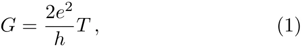
Firstly,we show the transmissions versus energy for quantum wire system of different sizes in Fig.2 and Fig.3.For comparison,the transmission of the corresponding uniform AGNR with the same width as the wire is also given.Generally,for a given energy,a uniform AGNR may allow several propagating modes that depends on its exact width,and each mode contributes unity to the transmission.Thus the total transmission is quantized and equals to the number of allowed propagating modes,which is shown in dashed lines in the two figures.As mentioned above,AGNRs can be either metallic or semiconducting depending on their exact widths,and have an energy gap when semiconducting.The energy gap width decreases with the increase of the width of the AGNR.Specifically,an AGNR composed with n rows of carbon atoms is metallic when n=3m+2 and is semiconducting otherwise,where m is an integer.The dashed lines in Fig.2 and Fig.3 refer to transmissions of metallic and semiconducting uniform AGNRs,respectively.
When we widen the two leads of an AGNR,a wire structure emerges.The translational symmetry of the system will be broken and the wire has fewer transverse modes than the leads.Electrons will be either re flected or transmitted at the interfaces between the leads and the wire due to the mismatching of transverse modes.Electrons transport from one lead through the wire to the other lead is effectively a quantum scattering process.Hence,the transmissions of the quantum wire systems exhibit fluctuations instead of platform structures increasing in steps of one.For a given energy,the maximum value of the transmission of the system is determined by the width of the narrowest part of the system,namely,the wire.We can see that the resonant peaks in the transmissions of the quantum wire system do not exceed the dash lines.In other words,widen the leads results in a decrease of the conductivity of the system due to the quantum scattering process.
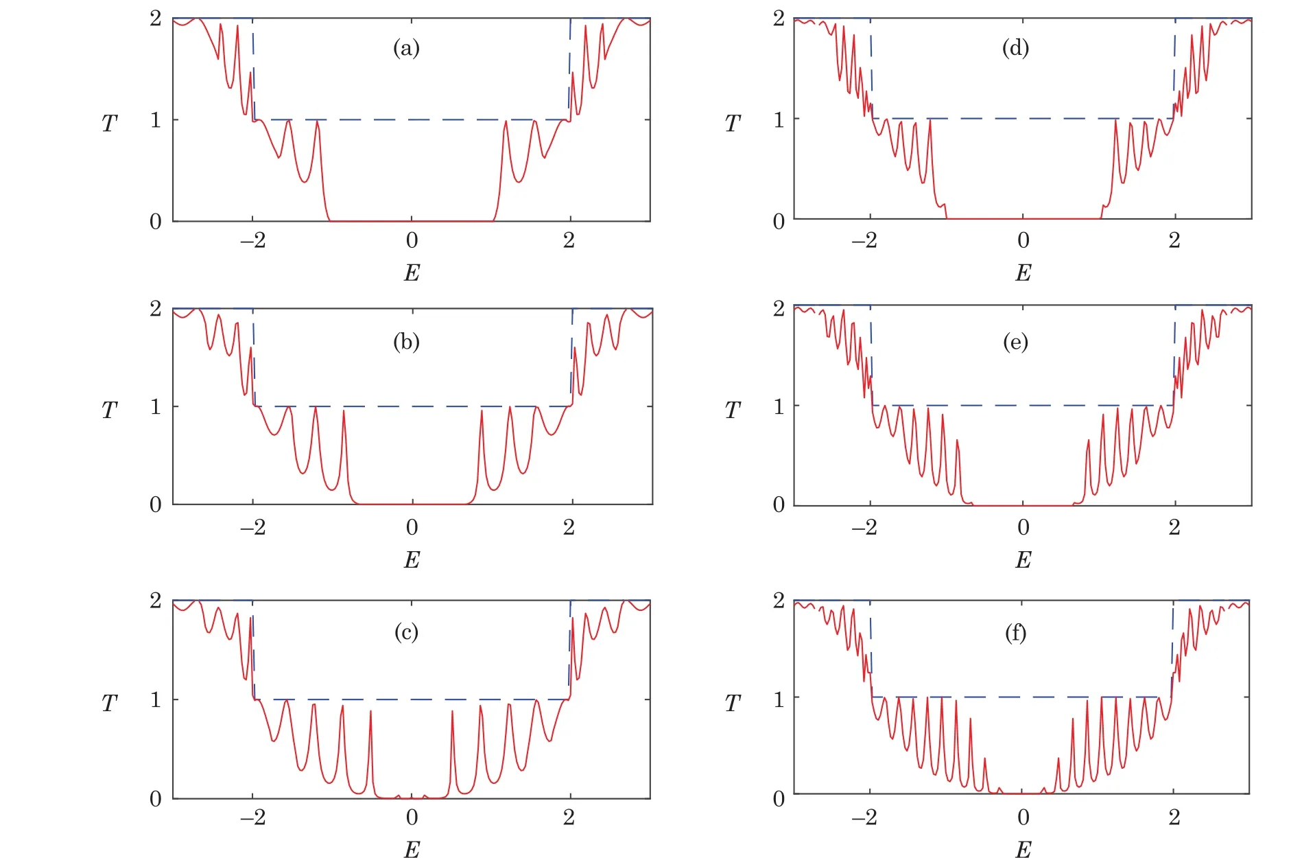
Fig.2 (Color online)Transmission versus energy for different graphene quantum wires when the wire is metallic(W0=2).(a)L0=10,W1=4;(b)L0=10,W1=6;(c)L0=10,W1=8;(d)L0=20,W1=4;(e)L0=20,W1=6;(f)L0=20,W1=8.The dashed line refers to transmission for the uniform AGNR with the same width as the wire.
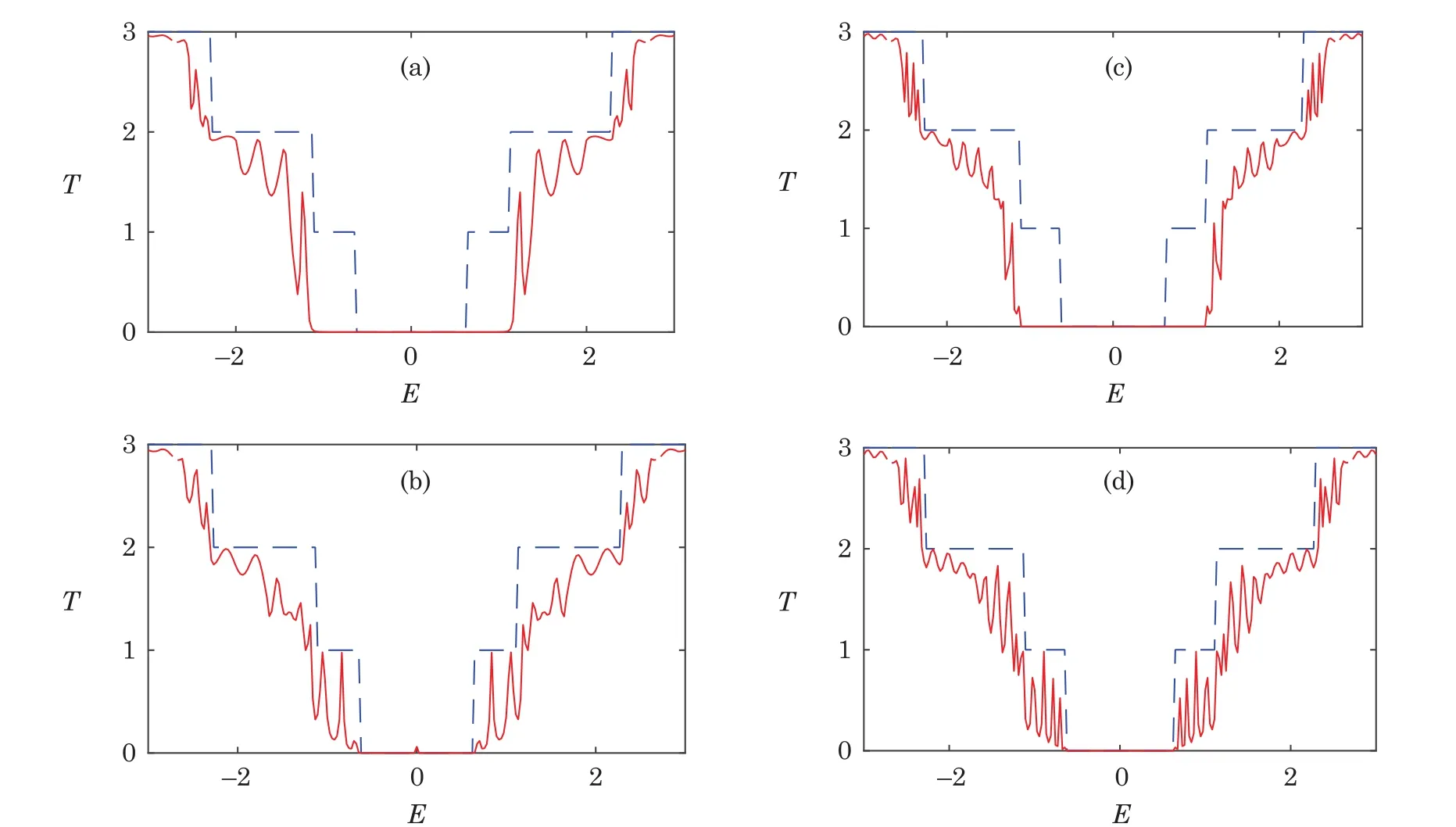
Fig.3(Color online)Transmission versus energy for different graphene quantum wires when the wire is semiconducting(W0=3).(a)L0=10,W1=5;(b)L0=10,W1=7;(c)L0=20,W1=5;(d)L0=20,W1=7.The dashed line refers to transmission for the uniform AGNR with the same width as the wire.
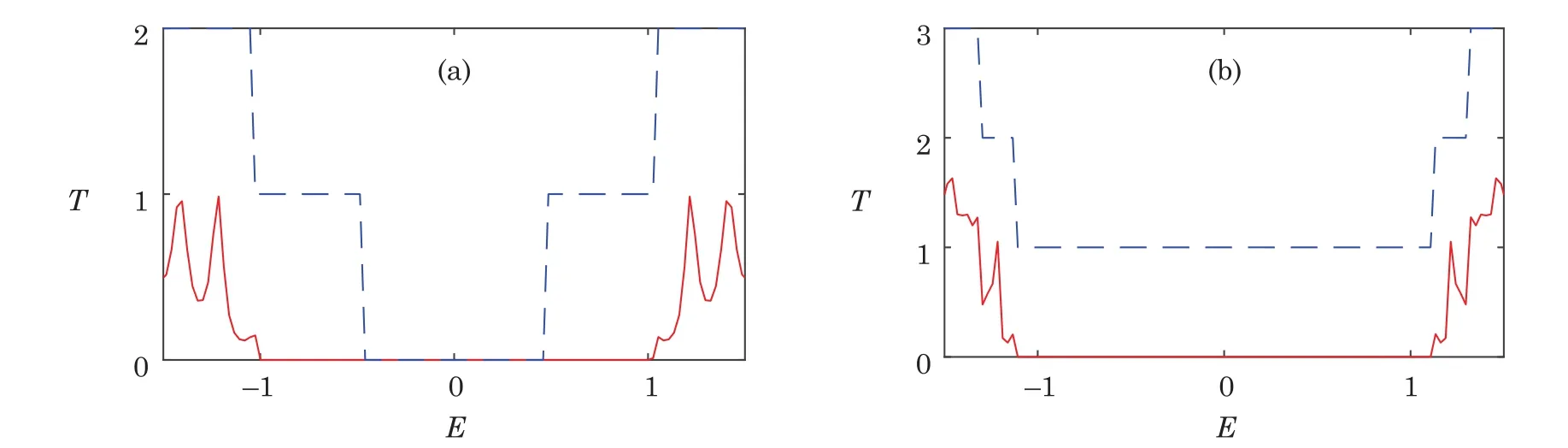
Fig.4 (Color online)Transmission versus energy for different graphene quantum wires in the region of low energy.(a)L0=20,W0=2,W1=4;(b)L0=20,W0=3,W1=5.The dashed lines refer to transmissions for uniform AGNRs with the same widths as the leads of the system.
The quantum scattering process also makes the transmission of the quantum wire system sensitively depends on its size.We first discuss the effect of the length of the wire L0on the transmission of the system.The left and right columns of graphs in Fig.2 and Fig.3 refer to transmissions of quantum wire systems with length L0=10 and L0=20,respectively.One can find that for fixed widths of the leads and the wire,increasing the length of the wire significantly intensifies the transmission fluctuations.The number of resonant transmission peaks increases with the increase of the wire length L0.The electron motion is governed by the Dirac equation for the graphene quantum wire.The resonant behavior of the electronic transmission arises from the interference of electronic wave functions inside the wire,[20]which travel forth and back due to the re flection between left and right contact-interface.As the length of the wire increases,more stationary states can be formed in the middle scattering region of the system.These states contribute to the transmission of the system and therefore increasing the length of the wire results in more remarkable fluctuations in the transmission curves.
Next,we investigate the in fluence of the width on the transport properties of the system.Graphs of the same columns in Fig.2 and Fig.3 correspond to graphene quantum wire structures with same fixed size central regions.While the widths of the leads for these systems are increased from top to bottom.It is found that,in general,the widths of the leads just slightly affect the amplitudes of the transmission peaks for the region of high energy.However,for the region of low energy,they have a significant in fluence on the transmission of the system.The energy gap around E=0 is still determined by the widths of the system,namely,the widths of the wire and leads.We proceed with the following discussions when the wire is metallic and semiconducting,as shown in Fig.2 and Fig.3,respectively.In Fig.2,the wire has n=5 rows of atoms and is metallic.There is no energy gap around E=0.However,when the leads become wider and are semiconducting(Figs.2(a),2(b),2(d)and 2(e)),an energy gap appears in the transmission spectrum.The width of the gap also decreases with the increase of the lead width.The energy gap only depends on the width of the system and is completely irrelevant to the length of the wire,which can be found by comparing Figs.2(a)and 2(b)with Figs.2(d)and 2(e),respectively.In Figs.2(c)and 2(f)we show the transmissions for the quantum wire systems when the leads are also metallic.One can find that tiny resonant transmission peaks appear around E=0 and the energy gap become narrow.This is because there exist allowed propagating modes around E=0 for both the leads and the wire.In Fig.3 we show the transmissions for the quantum wire system when the wire is semiconducting,while the leads are metallic(Figs.3(a)and 3(c))and semiconducting(Figs.3(b)and 3(d)).For a semiconducting wire,the energy gap can exist stably as the widths of the leads increase,no matter the leads are semiconducting or metallic.In summary,when the wire or the leads is semiconducting,the system is semiconducting.This reveals that the energy gap is more likely to open up in the graphene quantum wire system.
Interestingly,the energy gaps for the quantum wires shown in(Figs.3(a)and 3(c))are visibly broadened compared with the corresponding uniform AGNR.By several further numerical calculations,we find that when one part of the system,the leads or the wire,is metallic while the other part is semiconducting,the width of the energy gap is determined by the leads.In order to highlight the energy gap,the transmissions versus energy only in the low energy region is shown in Fig.4.We give the transmission for quantum wire system when the wire is metallic while the leads are semiconducting in Fig.4(a).The other case is demonstrated in Fig.4(b).The transmissions for uniform AGNRs having same widths with the two leads of the system are plotted in dashed lines.One can find that,the transmission of the quantum wire system is zero in the energy interval where there exists no more than one propagating mode in the leads.This indicates that the first propagating modes of the leads can be totally blocked in the two cases mentioned above.This may be an effective way to open and broaden an energy gap for the graphenebased devices.
4 Conclusion
In conclusion,we have investigated the electron transport properties of graphene-based quantum wires using the tight-binding model and the non-equilibrium Green function method.The results show that the size of the system has a great effect on the transmission of the system.The transmission exhibits fluctuations because the shape of the whole system is non-uniform.The number of resonant transmission peaks is determined by the length of wire,while the width of the leads mainly in fluence the transmission in the region of low energy.The quantum wire system is more likely to show semiconducting phase and the energy gap is completely determined by the width of the system.For proper width of the leads,the energy gap can be broadened.These results may have potential applications in the designing of graphene-based devices.
杂志排行
Communications in Theoretical Physics的其它文章
- Mixed Local-Nonlocal Vector Schrödinger Equations and Their Breather Solutions∗
- Circular Semi-Quantum Secret Sharing Using Single Particles∗
- Existence and Dynamics of Bounded Traveling Wave Solutions to Getmanou Equation∗
- Runaway Directions in O’Raifeartaigh Models∗
- The 1/NcExpansion in Hadron Effective Field Theory∗
- Quasinormal Modes of the Planar Black Holes of a Particular Lovelock Theory∗