A 16-Channel high-resolution time and charge measurement module for the external target experiment in the CSR of HIRFL∗
2014-04-24ZHAOLei赵雷KANGLongFei康龙飞ZHOUJiaWen周家稳LIUShuBin刘树彬andANQi安琪
ZHAO Lei(赵雷),KANG Long-Fei(康龙飞),ZHOU Jia-Wen(周家稳),LIU Shu-Bin(刘树彬),and AN Qi(安琪),
1State Key Laboratory of Particle Detection and Electronics,University of Science and Technology of China,Hefei,230026,China
2Department of Modern Physics,University of Science and Technology of China,Hefei,230026,China
A 16-Channel high-resolution time and charge measurement module for the external target experiment in the CSR of HIRFL∗
ZHAO Lei(赵雷),1,2KANG Long-Fei(康龙飞),1,2ZHOU Jia-Wen(周家稳),1,2LIU Shu-Bin(刘树彬),1,2and AN Qi(安琪)1,2,†
1State Key Laboratory of Particle Detection and Electronics,University of Science and Technology of China,Hefei,230026,China
2Department of Modern Physics,University of Science and Technology of China,Hefei,230026,China
High precision time measurement is required in the readout of the neutron wall and TOF walls in the external target experiment of the Cooling Storage Ring(CSR)project in the Heavy Ion Research Facility in Lanzhou(HIRFL).Considering the time walk correction,both time and charge are measured in the readout electronics.In this 16-channel measurement module,time and charge information are digitized by TDCs at the same time based on the Time-Over-Threshold(TOT)method;meanwhile,by employing high-density ASIC chips,the electronics complexity is effectively reduced.Test results indicate that this module achieves a time resolution better than 25ps and a charge resolution better than 5%over the input amplitude range from 50mV to 3V.
Time and charge measurement,Time-Over-Threshold(TOT),Photomultipliers tube(PMT),Cooling Storage Ring(CSR)
I.INTRODUCTION
The Cooling Storage Ring(CSR)project is the postacceleration system of the Heavy Ion Research Facility in Lanzhou(HIRFL).It consists of a main ring(CSRm)and an experimental ring(CSRe)[1,2].At the CSR complex,there exist an internal target experiment for hadron physics and an external target experiment for heavy ion collisions.The external target experiment is composed of one start time(T0) detector,oneγdetector,one big dipole,one neutron wall, six Multi-Wire Drift Chambers(MWDCs),and three Time of Flight walls(TOF walls),as shown in Fig.1.
As shown in Fig.1,the three TOF walls are placed in different angles to detect the time of f l ight of the charged particles from the collisions on the target.Time measurement is also required in the readout of the neutron wall,to determine the energy and emitted angle of the neutrons from the collisions. As for the TOF walls and the neutron wall,a time resolution as high as 25ps is required in the readout electronics[3].To guarantee a good time resolution,the leading edge discrimination method is employed;accordingly,charge information is also measured for time walk correction.Plastic scintillators accompanied by photomultipliers tubes(PMTs)are used in these two types of detectors.A typical waveform of the output signal from the PMT is shown in Fig.2,in which the leading edge is around 3ns.
A high-resolution time and charge measurement module(TCMM)is designed for the readout of both the TOF walls and the neutron wall.16 readout channels are integrated in each module which is based on the PXI(PCI eXtensions for Instrumentation)[4]standard to guarantee a high transfer rate.

Fig.1.(Color online)Detector system of the CSR external target experiment.
II.ARCHITECTURE OF THE TIME AND CHARGE MEASUREMENT MODULE
The structure of the TCMM is shown in Fig.3.The signal from the PMT is buffered and then split into two paths;one is imported to a discriminator for time measurement,and the other is transmitted to an SFE16 chip[5]for charge measurement,which is a charge-to-time converter(QTC).The HPTDC chip[6]is employed in this module for the digitization of the time information.Based on the time-over-threshold(TOT) method[7,8],the time and charge information(corresponding to the pulse width from the QTC)can be digitized at the same time.By use of multi-channel ASIC chips,a high integrity is achieved.
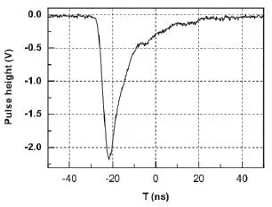
Fig.2.Typical waveform of the PMT output signal.

Fig.3.(Color online)Block diagram of the 16-channel time and charge measurement module.
The FPGA is responsible for data accumulation and the hardware conf i guration,as well as monitoring the front end. To enhance the time measurement performance,the algorithms for the correction of the HPTDC’s integral nonlinearity(INL)[9,10]are also integrated in this FPGA.As for the data readout,this module is implemented based on the PXI-6U standard,for which a CPLD chip is used as the interface with a PCI core in it.
III.ANALOG FRONT END CIRCUITS
As aforementioned,both time and charge information are required to be measured.To achieve a good performance,the signal is manipulated and transmitted in a fully differential mode.As shown in Fig.4,the input signal is buffered and converted to a differential pair,and then split to two paths;one is for charge measurement(VqpandVqn),and the other is for time measurement(VtpandVtn).
The differential operational amplif i er THS4500 from Texas Instruments Corporation is employed as the kernel of the preamplif i cation circuits.By careful selection of the resistor values,a gain(VOD/Vin)of around 2 can be achieved;meanwhile, an equivalent impedance(Rin)of 50Ω is designed to implement impedance match,as expressed in
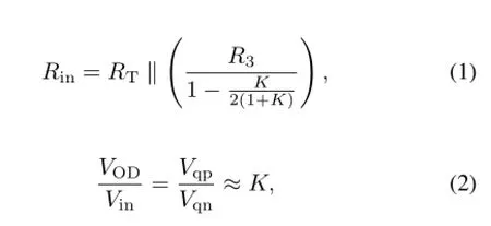
whereKis def i ned as

With the values of the resistors in Fig.4 and Eq.(1)to Eq.(3),the equivalent input impedance can be calculated to be 50Ω.
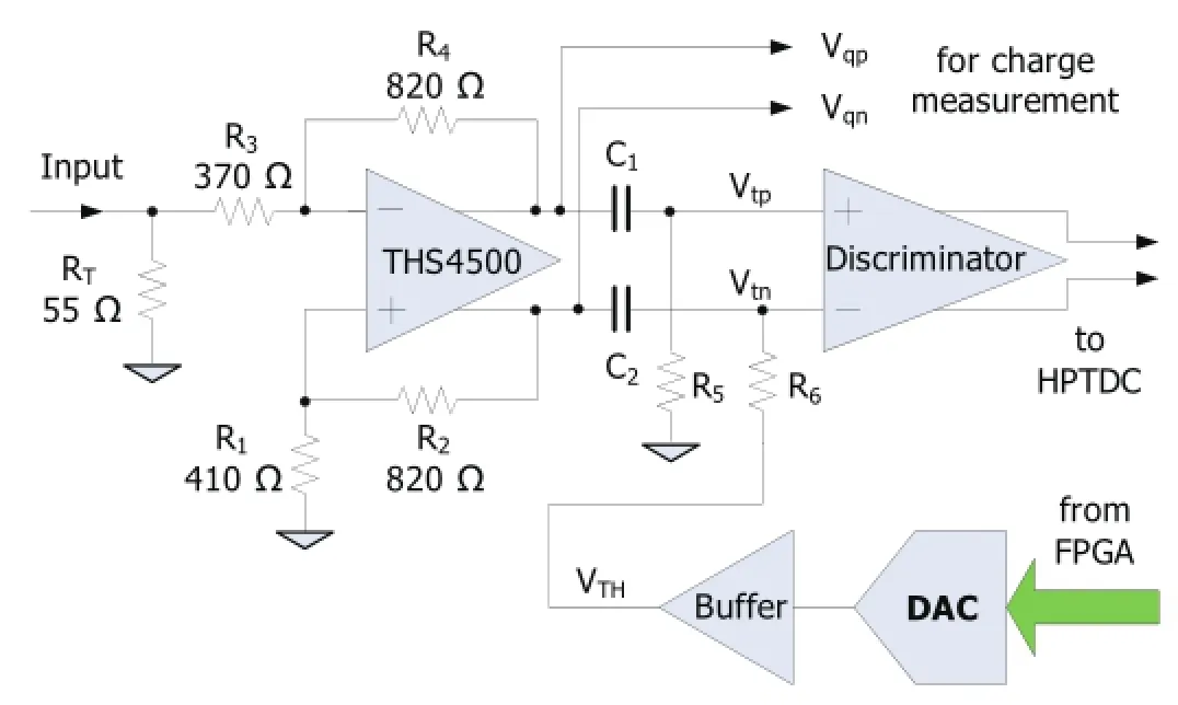
Fig.4.(Color online)Block diagram of the analog front end circuits for time measurement.
A serial input 12-bit DAC(AD7394)is used to generate the threshold voltage for the leading edge discrimination.An operational amplif i er is also used to enhance its driving ability.

Fig.5.(Coloronline)Signalwaveformsinthediscriminationprocess.
The signal waveforms for the time discrimination are shown in Fig.5.The input signal from the PMT is a negative pulse; through the analog front end,a pair of differential signals are generated and AC coupled,asVtpandVtnshown in Fig.5.The

Fig.6.(Color online)Block diagram of the analog front end circuits for charge measurement.

Fig.7.(Color online)Conf i guration and data readout of the chained HPTDCs.

Fig.8.(Color online)Block diagram of the logic design in the FPGA and CPLD.
baseline ofVtnis connected to the output of the DAC,which is actually set to the threshold voltage(VTH).The time information(T0)corresponds to the intersection of the curves ofVtpandVtn,with a voltage ofVTH/2 above the baseline ofVtp.We can also def i ne the signalVtD=Vtp−Vtn,andT0corresponds exactly to the threshold ofVTH.This fully differential process enhances the resistance to Electromagnetic Interference(EMI) and other common mode interference in the circuits.
As for the charge measurement,an ASIC chip(SFE16)is employed in this module.The front end circuits for the SFE16 are shown in Fig.6.The differential signalsVqpandVqnfrom the THS4500 in Fig.4 are converted to a single-ended signal, and the voltage amplitude of this signal is converted to a current signal throughR12,which is then imported to the SFE16 chip.As shown in Fig.6,the SFE16 consists of a charge sensitive amplif i er(CSA),a pole-zero cancellation(PZC)circuit,a shaper,a gain stage(×20),and a discriminator.Based on the TOT method,the charge information is converted to a pulse width which is afterwards digitized by an HPTDC.
IV.TIME-TO-DIGITAL CONVERSION
TheHPTDCisahighqualitytime-to-digitalconverter(TDC)chip designed by the micro-electronics group at CERN(European Organization for Nuclear Research)[10].It can work in four different modes,which are low resolution mode,middle resolution mode,high resolution mode and very high resolution mode.And the time resolution for each is 781ps,195ps,98ps and 24ps,respectively.In this design, two HPTDC chips(HPTDC#1 and#3 in Fig.7)are used in the very high resolution mode to achieve eight measurement channels with a resolution of 25ps;one HPTDC(HPTDC#2)is used to digitize the output pulse width of the SFE16,in which the high resolution mode(100ps)is employed.
To simplify the control and readout of the 3 HPTDCs,these chips are organized in a chain to obtain the conf i guration data via a common JTAG(Joint Test Action Group)port,as shown in Fig.7.Meanwhile,they share a parallel readout interface to transfer their data blocks in sequence by passing a token signal in a ring[11].

Fig.9.(Color online)System under test.
We use one FPGA chip(EP2C20F484 from Altera Cyclone II family)to process the data from the HPTDCs and function as the controller of this module.As shown in Fig.8,the SFE16 and the three HPTDCs are conf i gured by the FPGA withtheparametersstoredintheregisters,thecontentofwhich can be modif i ed by the remote PC.Since the TOT method is applied,the f i nal measurement results are time information from the HPTDCs.The input data streams are processed with the INL calibration logic and then buffered with an external SDRAM(MT48LC4M32).Two FIFOs marked as“FIFO1”and“FIFO2”function as the data bridge between different blocks.

Fig.10.(Color online)(a)INL test results;(b)Time resolution test results before and after calibration.

Fig.11.(Color online)(a)Typical histogram of time measurement results;(b)Time resolution of the 16 channels.

Fig.12.(Color online)(a)TOT output widths with different input signal amplitudes;(b)Charge resolution.
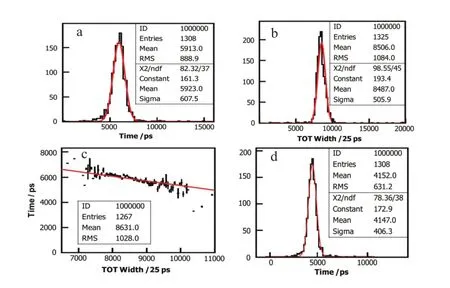
Fig.13.(Color online)(a)Time measurement results;(b)TOT output pulse width;(c)Relationship between time results and TOT widths;(d) Time measurement results after time walk correction.
V.LOGIC DESIGN
As for the data transfer interface,a CPLD chip is employed with a PCI core(pci mt32 from the Altera Company)[12]in it.A DMA engine is also used to implement the burst transfer. According to the test results,a data transfer speed more than 40MBps is achieved,in the situation of including the time cost of writing data to disks in the remote PC.
VI.TEST RESULTS
To evaluate the performance of this module,we conducted tests both in the laboratory and with the detectors.
A.Laboratory Test Results
Figure 9 shows the system under test.We used a signal source AFG3252 to generate the input signal according to the waveform shown in Fig.2.The clock module here is employed to provide clock signals(40MHz)for multiple measurement modules.The output data from the 16-channel TCMM are transferred to the remote PC for further analysis.
1.Time Measurement Tests
In the very high resolution mode of the HPTDC,its nonlinearity has direct inf l uence on the overall time measurement performance.In this design,the INL calibration is conducted to address this issue.The INL test results before and after the calibration are shown in Fig.10(a),which indicates signif i cant improvement.
We also conducted a series of tests to evaluate the time resolution before and after the calibration.The“cable delay test”method is used in this test.The signal source generates two output signals with a certain time delay,and then the RMS value of the time delay can be analyzed with a big amount of samples.Considering the situation that the time results of the two channels are not interrelated,the time resolution of single channel can be obtained by dividing the RMS value by 21/2.
As shown in Fig.10(b),with the INL calibration applied, the time resolution is enhanced to be better than 25ps.
Fig.11(a)shows a typical histogram of the time measurement results with the INL calibration applied.The typical time resolution(RMS)is 20.6ps.Wealso testedall the16 channels, the typical results of which are shown in Fig.11(b).Test results indicate that this module achieves a time resolution better than 25ps.
2.Charge Measurement Tests
We also conducted tests to evaluate the charge measurement resolution.With the TOT method applied,we can obtain the pulse width by directly subtracting the time points of the leading and falling edge of the output pulse from the SFE16.With the relationship between the input charge and output pulse width of the SFE16 chip,the charge information can be f i nally calculated.
In the tests,we changed the amplitude of the signal from the signal source,and got a series of test results.Fig.12(a)shows the TOT output widths with different input signal amplitudes,and Fig.12(b)shows the charge resolution from 50mV to 3V; in this input amplitude range,the charge resolution is better than 5%,beyond the requirement.
B.Initial Commissioning Test Results
After the tests in the laboratory,initial commissioning tests with the detectors were conducted in HIRFL.The plastic scintillators and PMTs are BC408(from Saint-Gobain Industrial Ceramics,Inc.)and R7527(from Hamamatsu),respectively. In the initial tests,cosmic rays are used as the input of the scintillator,and the output signal of the PMTs are measured by this TCMM.
Figure 13(a)shows the time measurement results,and TOT output signal widths(corresponding to charge information)are shown in Fig.13(b);Fig.13(c)is the relationship between the time results and TOT widths;Fig.13(d)shows the time measurement results after time-walk correction,and enhancement can be observed compared with Fig.13(a).The initial testing results concord well with the expected.Further commissioning tests will be conducted in future.
VII.CONCLUSION
A 16-channel high-resolution time and charge measurement module was designed for the readout of the TOF walls and neutron wall in the external target experiment in the CSR of HIRFL.By employing the TOT method,both time and charge information are digitized by the HPTDC chips.Test results indicate that this module achieves a time resolution better than 25ps and a charge resolution better than 5%over the input amplitude range from 50mV to 3V.
ACKNOWLEDGMENTS
TheauthorswouldliketothankXUHu-Shan,YUYu-Hong, and all of the CSR collaborators who helped this paper possible.
[1]Zheng C,Xiao Z,Xu H,et al.High Energ Phys Nuc,2007,31(12):1177–1180.
[2]Xia J,Zhan W,Wei B,et al.Nucl Instrum Meth A,2002,488: 11–25.
[3]Zhou J.Ph.D.Thesis,University of Science and Technology of China,2012.
[4]PXIHardwareSpecif i cationRevision2.2,Sept.2004. http://www.pxisa.org/userfiles/files/ Specifications/PXIHWSPEC22.pdf.
[5]Delagnes E,Abbon P,Bedfer Y,et al.IEEE T Nucl Sci,2000,47(4):1447–1453.
[6]Liu S,Guo J,Zhang Y,et al.Nucl Tech,2006,29(1):72–76.
[7]Manfredi P,Leona A,Mandelli E,et al.Nuclear Instruments and Methods in Physics Research A,2000,439:361–367.
[8]Liu X,Liu S,An Q.Nucl Sci Tech,2007,18(3):164–171.
[9]Liu S,Feng C,Yan H,et al.Nucl Sci Tech,2010,21:49–53.
[10]Zhou J,Liu S,Yin C,et al.Nucl Sci Tech,2011,22(6):372–378.
[11]Kang L,Zhao L,Zhou J,et al.Metrol Meas Syst(in press),DOI: 10.2478/mms-2013-0024.
[12]PCI Compiler User Guide,2005.http://www.altera. com/literature/ug/ug_pci.pdf.
10.13538/j.1001-8042/nst.25.010401
(Received July 22,2013;accepted in revised form December 2,2013;published online February 20,2014)
∗Supported by the Knowledge Innovation Program of the Chinese Academy of Sciences(No.KJCX2-YW-N27)and the National Natural Science Foundation of China(No.11079003)
†Corresponding author,anqi@ustc.edu.cn
猜你喜欢
杂志排行

Nuclear Science and Techniques的其它文章
- Feasibility study on optical vortex generation at Shanghai deep ultraviolet free-electron laser∗
- Lattice design and optimization of the SSRF storage ring with super-bends
- Temperature and carrier-density dependent excitonic absorption spectra of semiconductor quantum wires∗
- Bromate formation in bromide-containing waters irradiated by gamma rays∗
- Adsorption behavior of uranyl ions onto amino-type adsorbents prepared by radiation-inducedgraft copolymerization∗
- Radiation tolerance studies on the VA32 ASIC for DAMPE BGO calorimeter∗