Readout electronics for CSR-ETF silicon strip array detector system∗
2014-03-07ZHAOXingWen赵兴文QIANYi千奕KONGJie孔洁SUHong苏弘DUZhongWei杜中伟3ZHANGXueHeng章学恒YANDuo闫铎LIZhanKui李占奎LIHaiXia李海霞WANGXiaoHui王晓辉andTONGTeng童腾
ZHAO Xing-Wen(赵兴文),QIAN Yi(千奕),KONG Jie(孔洁),SU Hong(苏弘),,DU Zhong-Wei(杜中伟),,3ZHANG Xue-Heng(章学恒),YAN Duo(闫铎), LI Zhan-Kui(李占奎),LI Hai-Xia(李海霞),WANG Xiao-Hui(王晓辉),and TONG Teng(童腾)
1Institute of Modern Physics,Chinese Academy of Sciences,Lanzhou 730000,China
2University of Chinese Academy of Sciences,Beijing 100049,China
3State Key Laboratory of Particle Detectionamp;Electronics, University of Science and Technology of China,Hefei 230026,China
Readout electronics for CSR-ETF silicon strip array detector system∗
ZHAO Xing-Wen(赵兴文),1,2QIAN Yi(千奕),1KONG Jie(孔洁),1SU Hong(苏弘),1,†DU Zhong-Wei(杜中伟),1,3ZHANG Xue-Heng(章学恒),1YAN Duo(闫铎),1,2LI Zhan-Kui(李占奎),1LI Hai-Xia(李海霞),1WANG Xiao-Hui(王晓辉),1,2and TONG Teng(童腾)1,2
1Institute of Modern Physics,Chinese Academy of Sciences,Lanzhou 730000,China
2University of Chinese Academy of Sciences,Beijing 100049,China
3State Key Laboratory of Particle Detectionamp;Electronics, University of Science and Technology of China,Hefei 230026,China
A readout electronics has been developed for the silicon strip array detector system of HIRFL-CSR-ETF.It consists of 48 front end electronics(FEE)boards,12 PXI-DAQ boards and one trigger board.It can implement energy and time measurements of 4608 channels.Each FEE board is based on 6 ASICs(ATHED),which implements energy and time measurements of 96 channels.The PXI-DAQ board meets requirements of high-speed counting and amount of readout channels and can process signals of 4 FEEs.The trigger board is developed to select the valid events.The energy linearity of the readout electronics is better than 0.3%in the dynamic range of 0.1–0.7V.In the test with a standard triple alpha source,the energy resolution was 1.8%at 5.48MeV.This readout electronics enables the silicon strip array system to identify particles of A≤14.
Readout electronics,PXI-DAQ,Silicon strip,Front end electronics,Application specific integrated circuit
I.INTRODUCTION
Silicon strip detectors are widely used in nuclear physics, high energy physics,and astrophysics[1].Over the last 30 years,impressive developments were seen in silicon strip sensors and their readout electronics in high energy physics[2], due to parallel developments in electronics of low noise and very large system integration[3].Many special chips were developed for silicon strip detectors in different experiments, such as the ABCD3TA chip for the ATLAS tracker[4],the APV25 chip for the CMS tracker[5]and the A128C chip for the ALICE tracker[6].
A silicon strip array detector system will be equipped for the external target facility(ETF)of the Cooling Storage Ring on the Heavy Ion Research Facility in Lanzhou(HIRFLCSR-ETF)[1].It consists of twelve telescopes,each has two double-sided silicon strip detectors,and each detector is of 49.8mm×49.8mm,with 96 strips on each side.
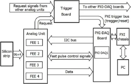
Fig.1.Block diagram of the readout electronics.
II.READOUT ELECTRONICS
The readout electronics for the silicon strip array detector system has 12 units.As shown in Fig.1,each unit consists of four identical FEE boards and a PXI-DAQ board.The trigger board is shared by 12 units.Each unit can implement energy and time measurements of 384 channels.So the readout electronics has energy and time measurements of 4608 channels.Each FEE board has six ASIC chips(ATHED),which are connected in daisy chain,and processes 96 channels of energy signals and 96 channels of time signals.This type of ASIC chip measures energy and arrival time of particles, and gives a trigger when the energy exceeds a minimum adjustable value[8].
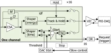
Fig.2.(Color online)Schematics of the ASIC.
The block diagram of ATHED is shown in Fig.2[8]. Briefly,ATHED is a 16-channel ASIC chip.Each ATHED channel includes a charge sensitive amplifier(CSA,11MeV, 22MeV,50MeV,100MeV and 200MeV),the energy branch(shaping at 1 and 3µs and track-and-hold),and the timing branch that consists of the fast shaping,discriminator with slow control,thresholds and time-to-amplitude converter(TAC,at 300 and 600ns)[8,9].The analogue energy and time information of 16 channels is transmitted through voltage-to-current converter(VIC)(±2mA/V)to the PXIDAQ board.ATHED improves the integration level of FEEs and enables multichannel data processing.ATHED is of good performances,and power dissipation of an ATHED channel is just 28mW,hence the reduced power dissipation of FEEs.
The PXI-DAQ board implements the slow control,analog output signal adapting,fast timing pulse generation,PXI interface communication and data acquisition.Each PXIDAQ board can process signals of 4 FEEs.To effectively reduce crosstalks between the FEE and PXI-DAQ boards, flat twisted-pair cables are used to transmit the low voltage differential signals(LVDS)[1].The trigger board makes a fast L1 trigger decisions.Also it generates trigger data that are packed and transmitted to PC via PXI bus for off-line analysis[10].The PXI platform-based readout system can satisfy requirements of high-speed counting and amount of readout channels[7].The software has a user-friendly GUI (Graphical User Interface)written in C language using Lab-Windows/CVI under Windows XP operating system[7].
A.Front end electronics board
As shown in Fig.3,the FEE board consists of six ASIC chips,an inner test pulse generator,a LVDS receiveramp; driver,and an inspection circuit.Each analog unit is composed of four FEE boards,which processes energy and time signals of 384 channels. The outputs of each board can be carried on one analogue differential-pair or on two analogue differential-pairs and the signals are sent in currentdifferential mode through twisted pair to the PXI-DAQ board. On each FEE,the programmable inner test pulse generator, whichdriveseachanaloguetestinputofeachATHED,checks the functionality of all the ASIC chips and implements physical calibration of each channel.
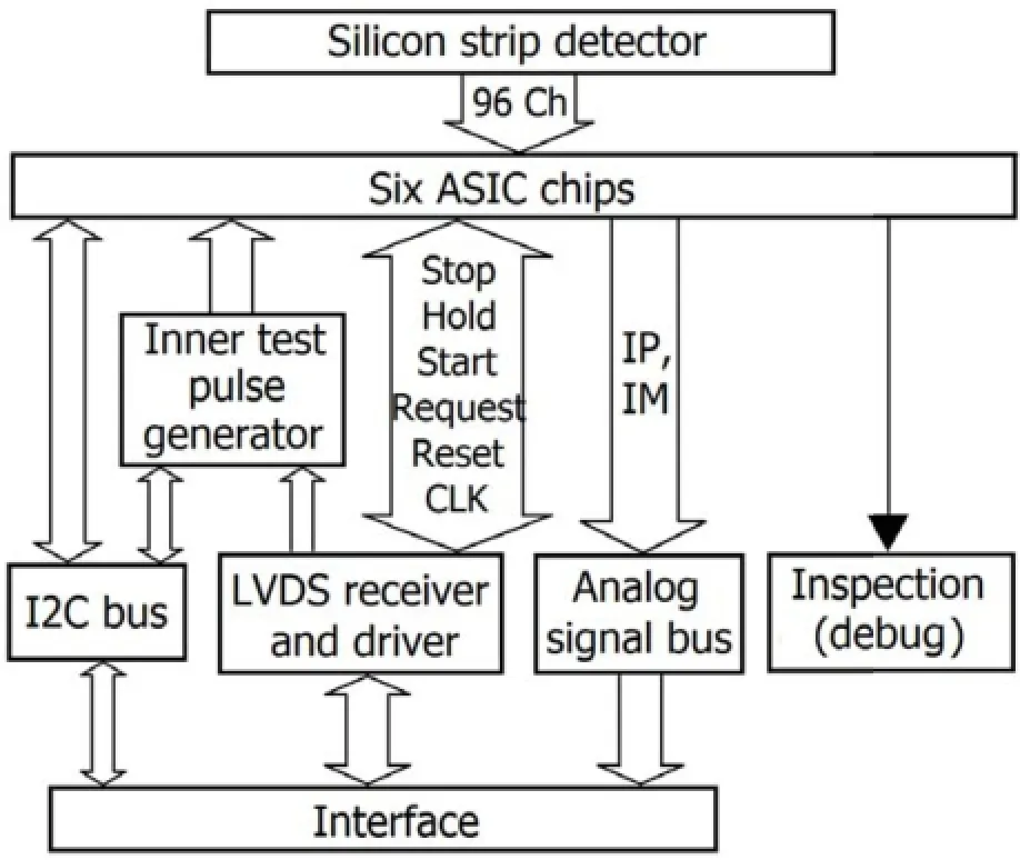
Fig.3.Block diagram of the analog unit.
The inner test pulse generator is based on PCA9555(16 bits I2C bus I/O port)and digital-to-analog converter(DAC). The output of the inner test pulse generator is used to inject a current signal to the input of a selected channel.With appropriate test signals,functionality of the ASICs can be tested by analyzing the data acquired by the PXI-DAQ.The debug signal generated by the ASIC is to check whether the ASIC chip works normally.
Against the electromagnetic interference(EMI),all the fast control signals(stop,hold,start,request,reset,CLK)are transmitted in LVDS standard.The request signals generated by the ASIC chips are transmitted to the trigger board for trigger signals pretreatment.The readout time of analog unit is less than 32µs when data are transmitted on two analogue differential-pairs and less than 61µs when data are transmitted on an analogue differential-pair.The transfer function for the silicon detector system is 34.22µA/MeV for each channel on the FEE board.
证明:设(u,a,b)满足关系式(3.1),由 J∂φ=(I+ρ∂φ)-1的定义,等式 成立,当且仅当

Fig.4.The timing diagram as data transmitted on an analogue differential-pair.
Figure 4 shows the timing diagram for data transmission on an analogue differential-pair.The energy information of a channel is transmitted to VIC at the rising edge of the CLK signal and the time information of a channel is transmitted to VIC at the falling edge of the CLK signal.The energy and time information of 96 channels,transmitted on an analogue differential-pair,is transmitted through VIC to the PXI-DAQ board channel by channel using 96 CLKs in total.Because data are transmitted at the rising and falling edge of the signal CLK,the signal Sclk is double frequency of the signal CLK. The signal Stop is transmitted to TAC and the signal Hold is transmitted to hold energy signals.
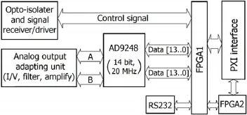
Fig.5.Block diagram of the PXI-DAQ unit.
B.PXI-DAQ board
The PXI plug-in DAQ board(Fig.5)consists of optoisolators,signal receiveramp;driver,analog output adapting unit,ADC,FPGA and PXI interface.Using four high-speed ADCs(20MHz),the PXI-DAQ can meet requirements of high-speed counting and amount of readout channels.A PXIDAQ board processes signals of 4 FEEs.In order to implement remote control,flat twisted-pair cables are used to transmit LVDS signals to effectively reduce crosstalks between the FEE and PXI-DAQ boards.To further reduce the crosstalks, the high-speed opto-isolators are used to block high voltages and voltage transients.After the I–V converter,low pass filtering and amplify circuit,the analog signals acquired from the FEE boards are fed into the high-speed ADCs(AD9248). Under control of the ADC converting sequence,digital signals are obtained,expressed with 14 bits binary number.If they are judged valid by FPGA,the digital signals will be packed with the event identification bits into a 32 bits frame, and stored into the FIFO,otherwise the signals are ignored. When the number of data stored in the FIFO exceeds the threshold set,an interrupt request signal is sent to the PXI bus for Master control.After that,the data in the FIFO are transferred to PC in DMA.Through the I2C bus interface, the PXI-DAQ board implements the parameter setting of the front-end ASICs,the test signal generator and other I2C components on the FEE boards.
C.Trigger board
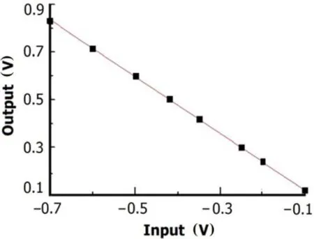
Fig.6.(Color online)The energy linearity of readout electronics over 0.6V range.
The trigger board receives request signals generated by the ASIC chips of FEE boards and makes fast L1 trigger decisions to select valid events.It generates the hold and reset signals and sends them via the trigger bus to the PXI-DAQ boards,which send the hold signals to the FEE boards to read data.The trigger board generates trigger data that are packed and transmitted to PC via PXI bus for off-line analysis[10].
III.PERFORMANCE OF THE READOUT ELECTRONICS
The readout electronics has been measured in the lab.The pulses generated by an ORTEC 448 pulser are transmitted to the test input of FEE board.The PXI-DAQ board sends the fast control signals to the FEE board after the trigger board gets the request signals generated by the FEE board.And meantime the PXI-DAQ board implements the data acquisition.As shown in Fig.6,energy linearity of the readout electronics is better than 0.3%in the dynamic range of 0.1–0.7V.Fig.7(a)shows the energy spectrum measured with the ORTEC 448 under laboratory conditions.The energy resolution is better than 0.5%(19MeV).Tested with a precision charge/time generator from Phillips Scientific(Model 7120), the time linearity is better than 0.2%in the dynamic range of 116–536ns.The time resolution is better than 0.24%in the range of 0–600ns.Fig.7(b)shows alpha spectrum of a standard triple alpha source(238Pu,241Am and244Cm)measured with a 49.8mm×49.8mm double-sided silicon strip detector system,for testing the readout electronics.
The energy resolution can be obtained through the Gaussian Fitting.As shown in Fig.7(b),the energy resolution is about 1.8%at 5.48MeV.The particle identification ability of the silicon strip detector can be estimated by Eq.(1).

where,δ(ΔE)/ΔE is energy resolution of the silicon strip detector,and the δE/E is energy resolution of a CsI detector, which is better than 3%generally[11].For a maximum value of δA=0.5,particles of A≤14 can be identified.As the silicon strip array detector is designed to identify the particles of A≤10,the readout electronics attains the goal of design.
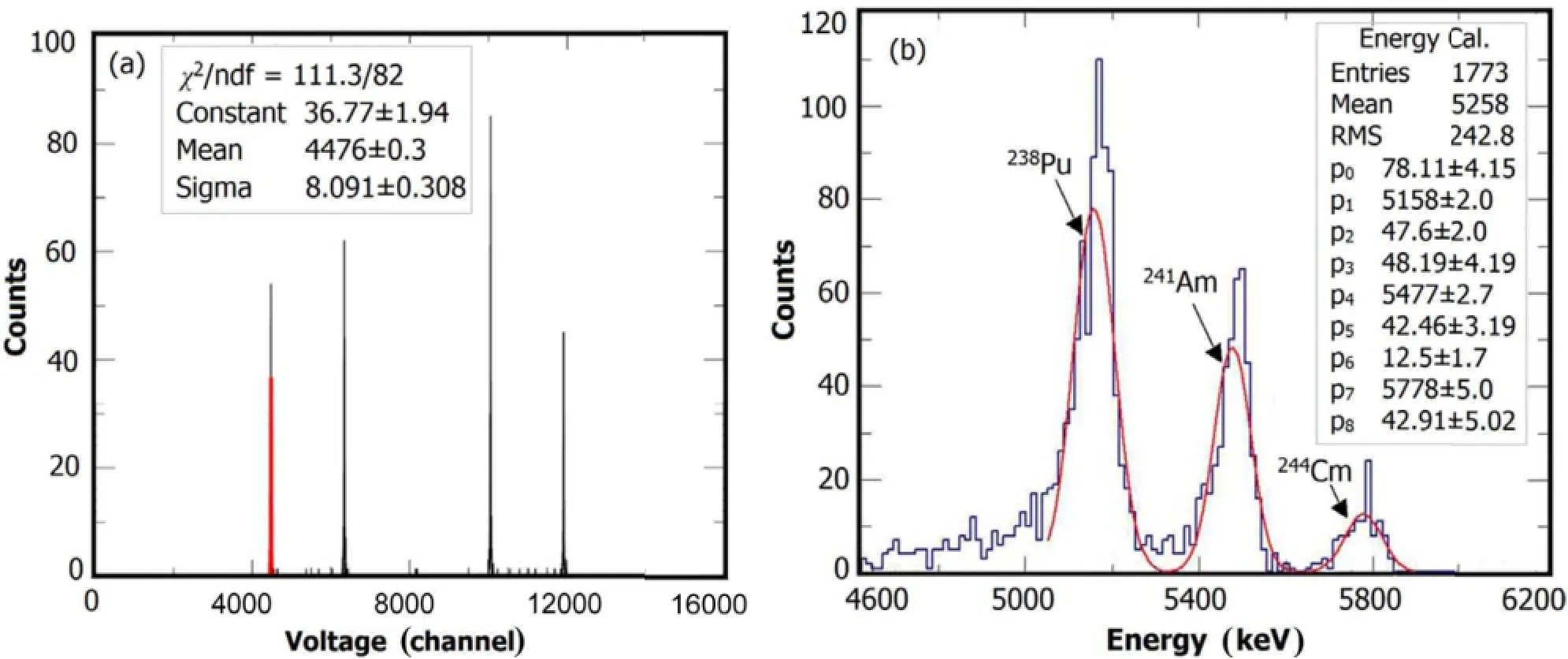
Fig.7.(Color online)Energy spectrum measured with ORTEC 448(a)and the silicon strip detector system(b).
IV.SUMMARY
A readout electronics system has been developed for CSRETF silicon strip array detector.It consists of 48 FEE boards, 12 PXI-DAQ boards and one trigger board.Using ASICs, the FEE implements the designs of high density,amount of readout channels and low power consumption.Using highspeed ADCs(20MHz),the PXI-DAQ board can implement quick acquisition of multichannel data.The readout electronics system can implement energy and time measurements of 4608 channels.And the system attains the desired purpose and is reliable for the nuclear physics experiments on ETF of HIRFL-CSR.
ACKNOWLEDGEMENTS
The authors would like to thank all the HIRFL collaborators for their support and useful suggestions.
[1]Qian Y,Su H,Kong J,et al.Chinese Physics C,2013,37: 016101.
[2]Won E,Choi J H,Ha H,et al.arXiv preprint arXiv:0704.1334.
[3]Monta˜no L M.Silicon microstrip detectors,AIP Conf Proc, 2006,857:143–151.
[4]Campabadal F,Fleta C,Key M,et al.Nucl Instrum Meth A, 2005,552:292–328.
[5]Raymond M,Cervelli G,French M,et al.The CMS Tracker APV25 0.25µm CMOS readout chip,Sixth Workshop on Electronics for LHC Experiments,CERN/LHCC/2000–041.
[6]Kuijer P.Nucl Instrum Meth A,2000,447:251–256.
[7]Kong J,Su H,Chen Z Q,et al.Nucl Instrum Meth A,2010, 622:215–218.
[8]Baron P,Atkin E,Blumenfeld Y,et al.IEEE Nucl Sci Conf R, 2003,386–390.
[9]Pollacco E,Atkin E,Auger F,et al.AIP Conf Proc,2006,831: 337–341.
[10]Du Z W,Su H,Qian Y,et al.arXiv preprint arXiv:1211.1087.
[11]Chen R F,Xu H S,Fan R R,et al.Chinese Physics C,2008, 32:135–138.
(Received November 15,2013;accepted in revised form March 16,2014;published online July 27,2014)
10.13538/j.1001-8042/nst.25.040402
∗Supported by the National Natural Science Foundation of China(Nos. 11005135 and 11079045),the Important Direction Project of the CAS Knowledge Innovation Program(No.KJCX2-YW-N27),and the Foundation of director of Institute Modern Physics,CAS(No.Y207170SZ0)†
,suhong@impcas.ac.cn
猜你喜欢
杂志排行

Nuclear Science and Techniques的其它文章
- Simulation studies on two-frequency RF gun
- Tidal effects on hydrostatic leveling system used in high precision alignment of particle accelerator∗
- External micro-PIXE analysis of Nd3+accumulation in Euglena gracilis∗
- Mass thickness measurements for dual-component samples utilizing equivalent energy of X-rays∗
- Synthesis of N,N′-dimethyl-N,N′-didecyl-3-oxa-diglycolamide for extraction of lanthanides∗
- A K-CELL injection system for SH-PermEBIT∗